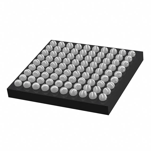
Cortex-M4 at 168 MHz in a WLCSP-90 footprint
The STM32F405OEY6BTR: Single-cycle multiply-accumulate and floating-point unit in a 90-ball WLCSP package measuring 4.22 x 3.97 mm.
168 MHz — what it buys for the control loop
At 168 MHz the Cortex-M4 core executes a 32-bit MAC or single-precision FPU operation in a single cycle.
512 KB Flash / 192 KB RAM — firmware staging and data buffers
The 512 KB of Flash is organized as 4 sectors of 128 KB each, which maps to a straightforward OTA update strategy: one sector for the bootloader, two for the active application image, and one for the rollback image. The 192 KB of SRAM splits into 128 KB of general-purpose RAM plus 64 KB of CCM RAM tightly coupled to the core. The CCM region has no bus matrix contention, so time-critical interrupt vectors and stack can live there while the main RAM handles DMA buffers for the ADC and USB.
Brown-out detect and POR are integrated, so an external supervisor is optional for most designs.
WLCSP-90 — layout and assembly considerations
The 90-ball WLCSP has a 0.4 mm pitch, which demands a controlled-impedance PCB stackup with microvias and a soldermask-defined pad. The package is lead-free compatible and rated MSL 3 — if the moisture-barrier bag has been open longer than the floor-life window, a 24-hour bake at 125°C is needed before reflow. The 4.22 x 3.97 mm body saves roughly 60% board area versus an LQFP-100, but the trade-off is that rework requires a hot-air station with a fine nozzle and a practised hand.