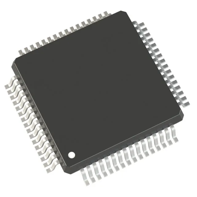
It carries 64 KB of Flash and 12K x 8 of SRAM — enough for a single motor-control FOC stack or a digital power converter with a few communication stacks, but tight for a GUI or a large data-logging buffer. The 21-channel 12-bit ADC and 3-channel 12-bit DAC give it a dense analog front-end for current sensing, voltage feedback, and analog setpoint generation without external converters. This part is aimed at industrial control, motor drives, power conversion, and sensor fusion applications where the combination of a DSP-capable FPU, fast 12-bit ADC, and CANbus connectivity matters more than raw memory density.
64 KB Flash — sizing the firmware budget
With 64 KB of Flash, the firmware engineer needs to budget carefully. A full sensorless FOC library plus CANopen stack can fit, but there is little room for a bootloader with dual-bank OTA.
The 64-LQFP package (10x10 mm body) is a hand-solderable, inspectable footprint with 51 usable GPIOs, which is generous for a 64-pin package.
The STM32F334 family shares a common die and pinout across density options, so if a future firmware growth requires more Flash, the STM32F334R8T6 (128 KB) or STM32F334C8T7 (64 KB, 48-pin) are drop-in software-compatible alternatives — same peripheral set, same register map, same toolchain.