72 MHz Cortex-M4 with HRTIM — what it does in a control loop
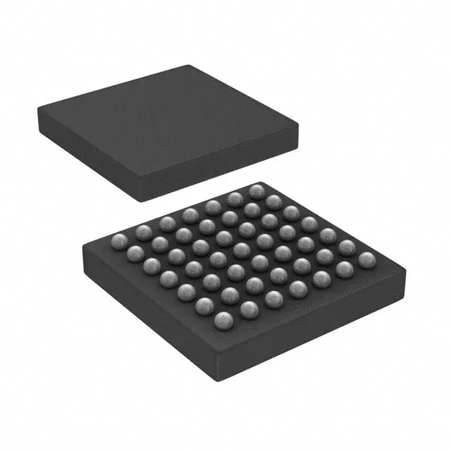
The STM32F334C8Y6TR: 64 KB of Flash and 12 KB of SRAM. 15-channel 12-bit ADC and three 12-bit DACs. 49-WLCSP (2.89 x 3.74 mm).
Memory and peripheral headroom for a BOM decision
64 KB of Flash and 12 KB of SRAM place this MCU in the value tier of the STM32F334 family. If your firmware needs a bootloader plus a moderate control loop, it fits. If you are adding OTA update staging or a full TCP/IP stack, the 64 KB Flash fills quickly — you will be looking at the 128 KB or 256 KB Flash siblings in the same package. The 37 I/O lines, CAN 2.0B, two SPI, two I²C, and five UART/USART interfaces cover most industrial sensor and actuator buses.
WLCSP package — layout and assembly reality
The 49-WLCSP (2.89 x 3.74 mm) is the smallest package option for the STM32F334C8. The 0.5 mm ball pitch and 0.3 mm ball diameter mean the PCB needs a fine-line capability — 0.1 mm trace/space minimum, microvia-friendly design. The exposed die backside is not a thermal pad; heat dissipation is through the solder balls and the board copper.