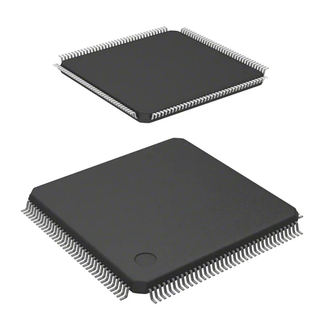
STMicroelectronics STM32F103ZGT6J — Microcontrollers & Processors (MCU / MPU / DSP)

STM32F103ZGT6J STM32F1 MCU, 72 MHz, 1 MB Flash, 144-LQFP

MPNSTM32F103ZGT6J
End of Life

STMicroelectronics STM32F103 series, ARM Cortex-M3, 32-bit MCU, STM32F103ZGT6J, 72 MHz, 1 MB Flash, 96 KB SRAM, 112 I/O, CAN/USB/SPI/I2C, 144-LQFP, -40°C to 85°C.

$0.5800Ref. price · indicative, final on quote
Independent supplier — new & surplus stockAuthenticity-screened · ESD-safe packingListing updated Jul 2026

Specifications

STM32F103ZGT6J specifications
ParameterValue
SeriesSTM32F1
MountingSurface Mount
Oscillator typeInternal
Program memory typeFLASH
Voltage - supply (Vcc (Vdd))2V ~ 3.6V
Operating temperature-40°C ~ 85°C (TA)
Speed72MHz
RAM size96K x 8
Core size32-Bit Single-Core
PackageTray
PeripheralsDMA, Motor Control PWM, PDR, POR, PVD, PWM, Temp Sensor, WDT
ConnectivityCANbus, I2C, IrDA, LINbus, SPI, UART/USART, USB
Number of i (O)112
Core processorARM® Cortex®-M3
Case144-LQFP
Data convertersA/D 21x12b; D/A 2x12b
Program memory size1MB (1M x 8)

Product details

It packs 112 I/O lines, a full set of connectivity peripherals — CANbus, USB, I2C, SPI, UART/USART, IrDA, LINbus — plus a 12-bit ADC (21 channels) and a dual 12-bit DAC. It is a workhorse part for motor drives, industrial PLCs, and embedded gateway designs that need a proven, well-documented MCU with ample Flash for complex firmware.

1 MB Flash and 96 KB SRAM — sizing the firmware budget

The 1 MB (1M x 8) Flash program memory is the high-density option in the STM32F103 line, giving room for a full RTOS, communication stacks (USB, CANopen), and application logic without external memory. The 96 KB SRAM supports moderate data buffering — enough for a 320x240 frame buffer or a CAN message queue — but designs needing large audio or image buffers should plan for external SRAM or a higher-RAM sibling. The Flash is read-while-write capable, so OTA updates are feasible with careful partitioning.

144-LQFP — rework and layout notes

The 144-LQFP (20x20 mm) is a 0.5 mm pitch package with 112 usable I/O. The exposed pad is not present on this QFP variant, so thermal dissipation goes through the leads — keep the trace widths adequate for the total package current limit.

The CANbus interface (one node) and USB full-speed device round out the connectivity for industrial gateway or data-logger roles.

For a BOM line, this means no near-term supply risk and full manufacturer support for new designs. The base product number STM32F103 spans multiple density and package variants, so a future migration to a smaller or larger Flash option stays within the same family and toolchain.

Frequently asked questions

What is the difference between STM32F103ZGT6 and STM32F103ZGT6J?

Both share the same 72 MHz Cortex-M3 core, 1 MB Flash, 96 KB SRAM, and 144-LQFP package. The functional ratings are identical; the choice is a logistics decision based on your assembly line's preferred media.

What is the maximum clock speed of STM32F103ZGT6J?

The maximum core clock speed is 72 MHz. At this frequency the Flash requires one wait state for zero-wait execution; the PLL can be configured from the internal oscillator or an external crystal. The 72 MHz limit is the same across the STM32F103 high-density line.