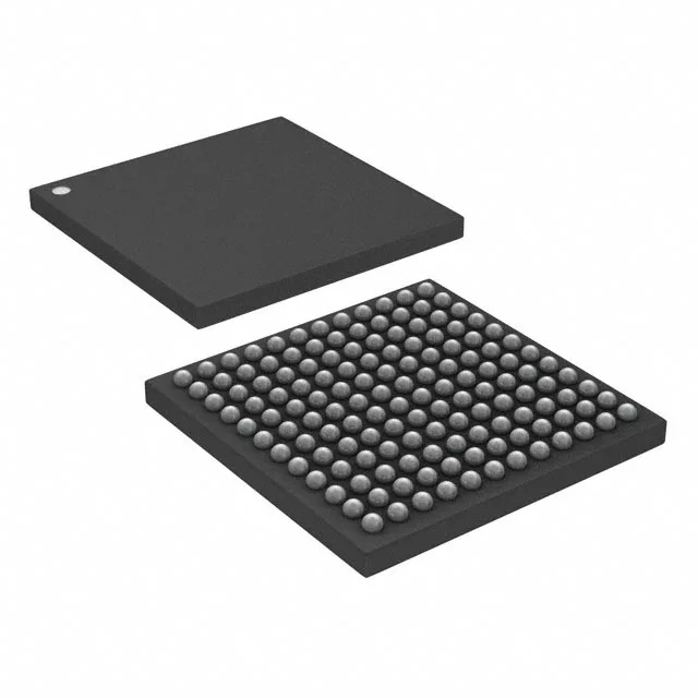
STMicroelectronics STM32F103ZEH7 — Microcontrollers & Processors (MCU / MPU / DSP)

STM32F103ZEH7 STM32F1 ARM Cortex-M3 MCU, 72 MHz

MPNSTM32F103ZEH7
Active

STMicroelectronics STM32F103ZEH7, STM32F1 series, 32-bit ARM Cortex-M3 MCU, 72 MHz, 512 KB Flash, 64 KB SRAM, 144-LFBGA (10x10), -40°C to 105°C, 2V to 3.6V supply, 112 I/O.

$12.9800Ref. price · indicative, final on quote
Independent supplier — new & surplus stockAuthenticity-screened · ESD-safe packingListing updated Jul 2026

Specifications

STM32F103ZEH7 specifications
ParameterValue
SeriesSTM32F1
MountingSurface Mount
Oscillator typeInternal
Program memory typeFLASH
Voltage - supply (Vcc (Vdd))2V ~ 3.6V
Operating temperature-40°C ~ 105°C (TA)
Speed72MHz
PackageTray
RAM size64K x 8
Core size32-Bit Single-Core
PeripheralsDMA, Motor Control PWM, PDR, POR, PVD, PWM, Temp Sensor, WDT
ConnectivityCANbus, I²C, IrDA, LINbus, SPI, UART/USART, USB
Number of i (O)112
Core processorARM® Cortex®-M3
Case144-LFBGA
Data convertersA/D 21x12b; D/A 2x12b
Program memory size512KB (512K x 8)

Product details

72 MHz Cortex-M3 with 512 KB Flash — the high-density tier

It is the high-density variant in the F103 line, designed for applications that need the full 512 KB code space and the 112 I/O count that the 144-ball BGA package enables. The core is a single Cortex-M3 with a 3-stage pipeline and hardware multiply/divide, clocked from an internal oscillator or an external crystal. For a BOM that needs the 144-ball BGA footprint and the 512 KB / 64 KB memory split, this is the production-grade MCU to specify.

On-chip peripherals include DMA, motor-control PWM, PDR (power-down reset), POR (power-on reset), PVD (programmable voltage detector), a temperature sensor, and a watchdog timer. The data converters give you 21 analog inputs at 12-bit resolution and two 12-bit DAC outputs.

144-LFBGA (10x10) — what the package means for the board

The 144-LFBGA package measures 10x10 mm with a 0.8 mm ball pitch. That is a fine-pitch BGA — the board needs a solder mask defined pad, a via-in-pad or microvia strategy for the inner rows, and X-ray inspection after reflow. The supplier device package code is 144-LFBGA (10x10). Surface-mount only, no through-hole equivalent. For rework, a hot-air station with a BGA nozzle and a preheater is mandatory — do not attempt with a soldering iron. The 112 I/O count means roughly 28 unused balls in a typical design, which can be left floating or tied to ground per ST's recommendation.

No lead-time or stock figures are held on this page; the quote will reflect real-time supply.

Frequently asked questions

Can the STM32F103ZEH7 work with a 5V supply?

The MCU cannot be powered from a 5 V rail. However, many I/O pins are 5 V tolerant — consult the STM32F103 reference manual for the specific pin mapping of 5 V tolerance.

Is there a direct replacement or equivalent for the STM32F103ZEH7?

Within the STM32F103 family, pin-compatible alternatives exist across the density and package options — for example, the STM32F103VET6 (100-pin LQFP) is a different footprint. For a true 144-BGA replacement with the same memory and peripheral set, the STM32F103ZEH7 is the correct order code. No direct second-source from another manufacturer is listed in this evidence.