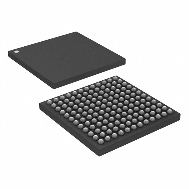
What this chip is — STM32F103ZEH6TR
This is the high-density, high-pin-count member of the F103 family — the one you pick when you need the full complement of peripherals and GPIO in a BGA footprint. It includes a full set of peripherals: DMA, multiple 12-bit ADCs, dual 12-bit DACs, motor-control PWM timers, and wired interfaces covering CAN, I²C, SPI, USART, and USB.
72 MHz Cortex-M3 — what the clock tree needs from firmware
The 72 MHz maximum core clock is the same across the STM32F103 high-density line. If you are bringing up firmware from scratch, the HSI internal oscillator gets you started but you will switch to the PLL for full speed. The flash controller needs one wait state above 48 MHz — skip that step and the first branch instruction after the PLL lock will hard-fault. SWD and the boot ROM stay alive regardless of the watchdog state, so recovery is straightforward even after a bad clock configuration.
512 KB of program Flash is enough for a full RTOS, a USB stack, CANopen or Modbus application layer, and a modest GUI framebuffer. The 64 KB SRAM splits into 48 KB of main SRAM and 16 KB of DMA-capable SRAM on the bus matrix — that second block is useful for holding ADC sample buffers or Ethernet descriptors without contention. If your application needs more than 64 KB of RAM at runtime, this part will force an external memory add-on or a move to the STM32F2/F4 series.
144-ball LFBGA — layout notes for the BGA footprint
The 144-LFBGA package is a 0.8 mm pitch BGA, roughly 10 x 10 mm body. The ball map follows the standard STM32F103 high-density pinout, so the same PCB footprint works for the STM32F103Vx (100-pin LQFP) only after a complete redesign — these are not drop-in compatible. Fanout is manageable with a 4-layer board; a 2-layer board is possible if you route the inner balls carefully, but the BGA's center balls (VDD, VSS, and some I/O) make it tight. Use via-in-pad or at least a 0.3 mm via with tenting for the inner rows.
Connectivity and analog — what the peripherals cover
The peripheral set is comprehensive for a mid-range MCU: three 12-bit ADCs with up to 21 multiplexed channels, two 12-bit DACs, and a motor-control timer with six complementary PWM outputs. On the digital side you get CAN 2.0B, two I²C, three SPI, five USARTs (all with IrDA and LIN support), and a USB 2.0 full-speed device. The DMA controller has 12 channels and can service ADC, timer, SPI, I²C, and USART without CPU intervention — essential for keeping the core free to run the application logic.