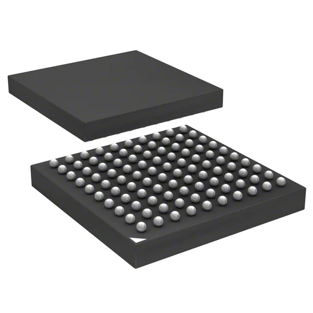
72 MHz ARM Cortex-M3 with 512 KB Flash in a 100-ball BGA
The STM32F103VEH7: 80 I/O lines, CAN, USB, I²C, SPI, UARTs, motor-control PWM timers, and dual 12-bit DACs.
100-LFBGA — footprint and rework considerations
The 80 I/O are distributed across the ball array; the centre pads are typically VDD and VSS, so decoupling capacitors should be placed on the bottom layer directly under the BGA footprint.
The base product number is STM32F103, which shares the same die and peripheral set across the density and package variants, so a PCN affecting the series would apply uniformly.
Peripheral set — motor control and CAN on a single chip
The integrated motor-control PWM timers, together with the 12-bit ADC (16 channels) and dual 12-bit DAC, make this MCU a natural fit for field-oriented control of brushless DC motors. The CAN 2.0B interface connects directly to industrial automation backbones or automotive powertrain networks. The USB 2.0 full-speed device interface, along with I²C, SPI, and five UART/USART ports, covers most sensor-fusion and human-machine-interface communication needs without external bridge chips.