72 MHz Cortex-M3 — enough for most real-time loops
The 72 MHz core clock is the performance ceiling for the STM32F1 family. With a single-cycle multiply and a 12-cycle divide, it handles PID loops, Modbus polling, and sensor fusion comfortably. If you are coming from an 8-bit or 16-bit MCU, the jump to 32-bit at this speed usually means you can consolidate several tasks into one chip. The flash prefetch buffer helps keep the pipeline fed without wait states at 72 MHz, but if you push the PLL from a low-speed external crystal, bump the flash latency to 1 wait state before raising the core clock — the hard-fault on first branch is a classic bring-up trap.
100-ball BGA — plan the rework flow
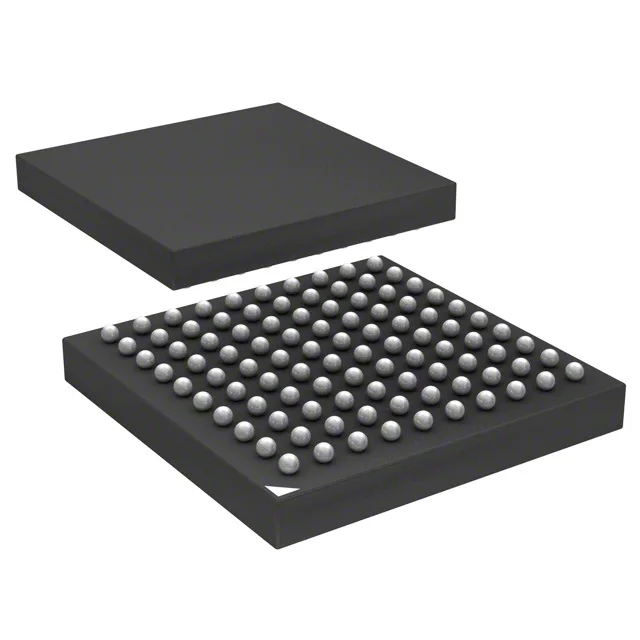
The 100-LFBGA is a fine-pitch BGA (0.8 mm ball pitch typical for this package size). It saves board area compared to an LQFP-100, but it means you need X-ray inspection and a rework station with a bottom-side preheater. The 80 I/O pins fan out across the ball grid, so route the decoupling caps close to the BGA vias on the back side; the core draws transient current on every clock edge.
Peripheral set: CAN, USB, and a dozen serial ports
This part includes CANbus, USB (full-speed device), SPI, I2C, IrDA, LINbus, and multiple UART/USART channels. That is enough to wire up a motor drive with CANopen, a USB-to-serial debug link, and a handful of I2C sensors without external UART bridges. The two 12-bit DACs and the 16-channel 12-bit ADC cover analog output and multi-sensor acquisition. The motor-control PWM timer with complementary outputs and dead-time insertion is there for BLDC or PMSM drives — no external PWM generator needed.
Lifecycle: active, no LTB pressure
The STM32F1 series is mature and widely second-sourced through the ecosystem, though no official pin-compatible alternate is listed here.