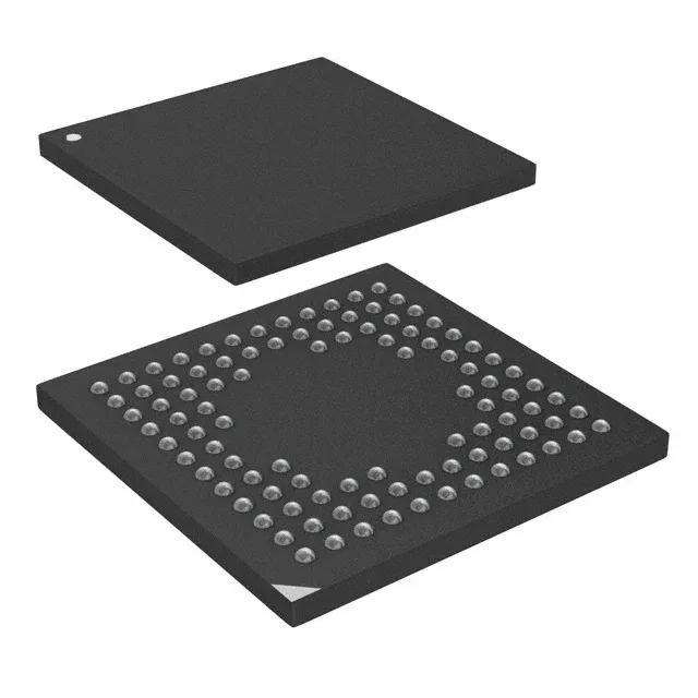
The STM32F103VBI6TR: The 72 MHz ARM Cortex-M3 core is the throughput ceiling for this MCU. At this speed, the part can handle a real-time control loop with a few hundred microseconds of headroom, run a lightweight protocol stack (CANopen, Modbus, USB device), and still leave MIPS for background tasks. The 128 KB Flash and 20 KB SRAM are sized for mid-range firmware — a motor-control algorithm with field-oriented control, a sensor hub aggregating SPI and I²C data, or a simple HMI with a small frame buffer. If the application needs more than 20 KB of RAM for data logging or a larger protocol buffer, this part will run out of headroom; that is the first fit check for the BOM line.
100-UFBGA (7x7) — compact footprint, different rework rules
The 100-UFBGA (7x7) package is the key differentiator from the more common LQFP variants. It saves board area — the 7x7 mm body is smaller than a 100-pin LQFP — but it is a BGA, so the PCB needs a via-in-pad or microvia stackup, and rework requires a hot-air station with a BGA nozzle and a preheat plate.
Peripheral set — CAN, USB, SPI, I²C, UART
The connectivity block includes CANbus, USB, SPI, I²C, UART/USART, IrDA, and LINbus — enough to talk to most industrial sensors, motor drives, and human-machine interfaces without an external bridge chip.