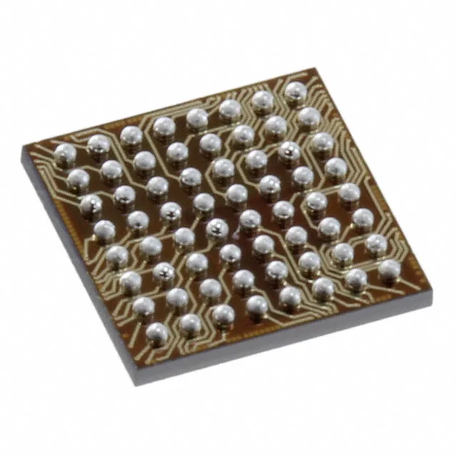
It comes in a 64-pin wafer-level chip-scale package (64-WLCSP, 4.47×4.4 mm), which is the smallest footprint option in the high-density STM32F103RE line — useful where board area is tight but you still need the full peripheral set: DMA, motor-control PWM, CAN, multiple UART/SPI/I²C interfaces, a 16-channel 12-bit ADC, and a 2-channel 12-bit DAC.
At 72MHz, the ARM Cortex-M3 core delivers around 1.25 DMIPS/MHz, so about 90 DMIPS peak. That's enough for real-time control loops in motor drives (the part has dedicated PWM timers), sensor fusion, or protocol bridging between CAN and USB without an external processor. The 512KB Flash means the firmware can carry a full communication stack (USB CDC, CANopen) plus application code without squeezing into a smaller density tier. The 64KB SRAM is adequate for moderate data buffering; if your application needs frame buffers or large lookup tables, check whether the RAM fits or you need the STM32F103ZG with 96KB.
WLCSP package — layout and assembly considerations
The 64-WLCSP (4.47×4.4 mm) is a direct-solder-ball package with no peripheral leads — all 51 I/O plus power and ground are under the body on a 0.4 mm or 0.5 mm ball pitch (confirm the specific ball map from the STM32F103RE datasheet). Not a package for prototype hand-assembly; plan for panelized production runs with stencil and pick-and-place.