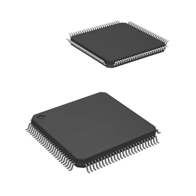
The STM32F101VCT6TR: The part includes a 12-bit ADC (16 channels) and a 12-bit DAC (2 channels), plus peripherals such as DMA, PWM, a temperature sensor, and multiple watchdogs.
The 36 MHz ARM Cortex-M3 core delivers roughly 0.9 DMIPS/MHz, or about 32 DMIPS total. That is half the clock of the STM32F103 sibling (72 MHz), so this part targets control loops and data logging rather than high-speed DSP or heavy protocol stacks. The 256 KB Flash is adequate for moderate firmware images; the 32K x 8 SRAM (32 KB) supports a modest RTOS or bare-metal state machine with a few communication buffers. If your application needs more headroom, the STM32F103VCT6 (same pinout, double the clock, plus USB and CAN) is the natural upgrade path.
The 100-LQFP (14x14 mm) with 0.5 mm pitch is a standard fine-pitch QFP — hand-reworkable with a hot-air station and some flux, but the 0.5 mm pitch demands a steady hand and a good stencil for reflow. The exposed pad (if present — check the mechanical drawing) is not a thermal pad; it is tied to VSS and should be soldered down for mechanical stability, not heat dissipation.
For dual-sourcing resilience, the pin-compatible STM32F103VCT6 is an official second source within the same family — though it adds USB, CAN, and a 72 MHz core, so firmware and clock-tree changes are required.