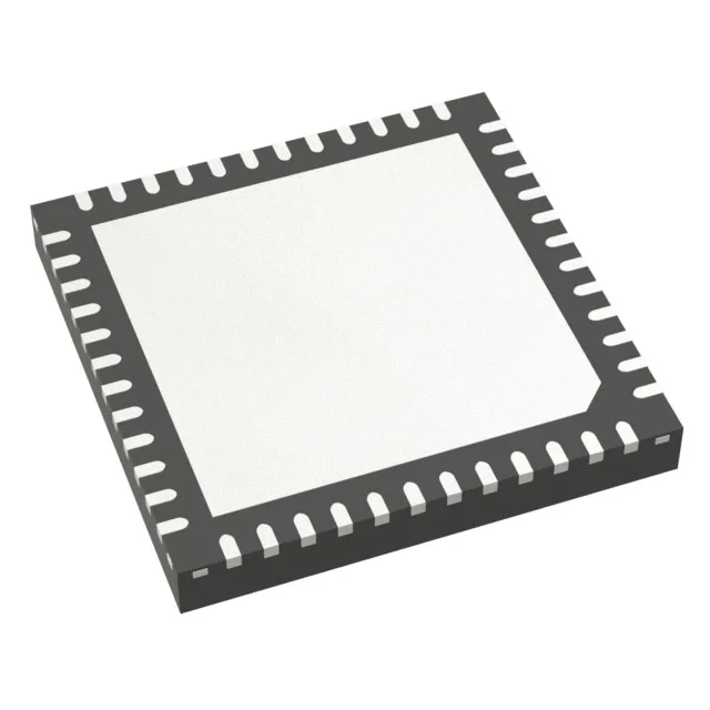
The STM32F101CBU6: The 36 MHz maximum clock speed places this MCU in the low-to-mid performance tier of the Cortex-M3 family. The flash wait state configuration is straightforward — at 36 MHz with a 2V to 3.6V supply, zero wait states are sufficient for most accesses; the STM32F1's prefetch buffer helps keep the pipeline fed. For firmware engineers: the internal oscillator is available, but an external crystal improves accuracy for USB-less UART baud-rate generation.
Memory sizing — 128 KB Flash, 16 KB RAM
128 KB of program Flash and 16 KB of SRAM set a clear boundary for firmware scope. The Flash is sufficient for moderate-sized application code, a bootloader, and a small real-time operating system kernel. The 16 KB RAM must be allocated carefully — stack, heap, and DMA buffers share this space. If the application uses the 12-bit ADC with double-buffered DMA transfers or a TCP/IP stack (via external PHY and SPI), the RAM budget becomes tight. The 16 KB RAM is organized as 16K x 8 bits; there is no separate EEPROM array — data that must survive reset should be stored in a reserved Flash sector with wear-leveling.
I/O and peripheral complement
With 37 general-purpose I/Os available from the 48-pin package, the STM32F101CBU6 can handle a mix of digital inputs, PWM outputs, and serial interfaces. The peripheral set includes two SPI, two I²C, and three USART channels (plus IrDA and LIN modes), which covers common sensor and actuator links in industrial designs. The 10-channel 12-bit ADC samples at up to 1 µs conversion time — adequate for monitoring analog signals like thermocouples or potentiometers at moderate update rates. The DMA controller can offload data transfers between peripherals and memory without CPU intervention, reducing interrupt overhead.
The exposed pad is electrically connected to VSS — it must be soldered to the board ground pour.
For dual-sourcing resilience, the STM32F101 series is pin-compatible across the 48-pin UFQFN package variants within the same density tier — the STM32F103CBU6 (same package, 72 MHz, more peripherals) is a functional upgrade if the application can absorb the higher clock and cost.