24 MHz Cortex-M3 — the value-line workhorse
Why 24 MHz matters for your BOM
The 24 MHz core speed is the key differentiator between the STM32F100 value line and the mainstream STM32F103 line, which runs at 72 MHz. For cost-sensitive control loops — reading a sensor, updating a PWM duty cycle, or managing a UART protocol — 24 MHz is often enough, and the lower clock reduces power draw and EMI. But if your application needs heavy number crunching, fast data logging, or high-speed communication, the 24 MHz ceiling will be the bottleneck. Match the clock to the task: this part fits where the STM32F103 would be overkill.
Memory budget — 512 KB Flash, 32 KB RAM
512 KB of Flash is generous for a value-line MCU; it can hold a full application stack including a real-time OS, communication stacks, and application code. The 32 KB RAM is more modest — budget carefully for buffers, stack, and dynamic data. If your design uses large frame buffers or extensive data logging, you may need to move data to external SRAM or select a part with more RAM. The Flash is organized as 512 KB (512K x 8), which is typical for STM32F1 devices in this density tier.
Analog integration — 16x12-bit ADC and 2x12-bit DAC
With 16 multiplexed 12-bit ADC channels and two 12-bit DAC outputs, this MCU can handle multiple analog inputs (temperature, pressure, current sense) and generate analog control signals (setpoint, reference) without external converters. The 12-bit resolution is adequate for many industrial and consumer applications; if you need higher precision (e.g., 16-bit), plan for an external ADC. The ADC and DAC share the same supply rails, so noise on the VDD line will affect conversion accuracy — keep the analog supply clean.
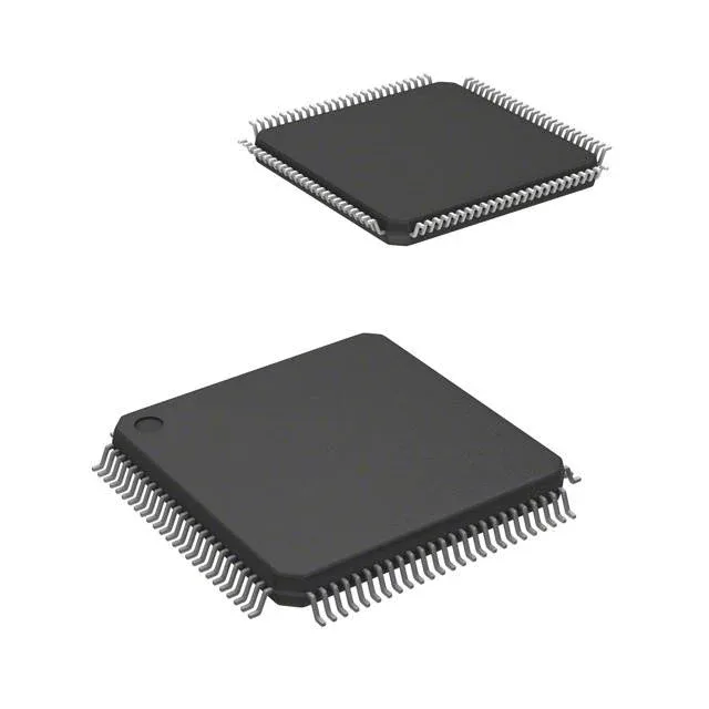
Package and rework — 100-LQFP, 14x14 mm
The 100-LQFP package (14x14 mm) is a standard, rework-friendly footprint. The leads are exposed on all four sides, so hot-air rework is straightforward — lift the part, not the pad. The 100-pin count gives 80 I/O, which is ample for most control applications.