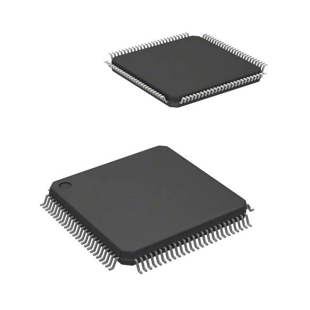
The 384 KB Flash (organized as 384K x 8) gives you room for a full application stack — RTOS kernel, communication protocol libraries, and application code — without immediately needing external memory. The 32K x 8 SRAM is adequate for moderate-sized data buffers and stack usage; if your design runs heavy frame buffers or large lookup tables, budget for external SRAM or a part with more on-chip RAM. The Flash is field-reprogrammable, so firmware updates over I2C, SPI, or UART are feasible with a bootloader in the reserved sector.
Supply range 2V to 3.6V and industrial temperature grade
The wide Vcc range of 2V to 3.6V means this MCU can run directly from a 3.3V rail or from a 2V battery-backed supply without an external regulator — useful for low-power or backup modes.
Integrated peripherals — ADC, DAC, DMA, and communication interfaces
The 16-channel 12-bit ADC and 2-channel 12-bit DAC let you digitize sensor inputs and output analog control signals without external converters — a real BOM consolidation for analog control loops. DMA offloads the CPU for peripheral-to-memory transfers, which matters when servicing multiple UART or SPI streams simultaneously. Connectivity includes I2C, SPI, UART/USART, and IrDA and LINbus for automotive or industrial bus interfaces. The PVD (programmable voltage detector) and POR/PDR circuits provide built-in brown-out protection, reducing the need for external supervisory ICs.