What the 24 MHz core speed means for your design
The 24 MHz maximum is the defining performance ceiling of this device — it is roughly one-third the speed of the mainstream STM32F103 series. That makes the STM32F100RDT7B a fit for control-loop, sensor-fusion, and human-interface tasks where throughput is not the bottleneck. If your application needs faster math or tighter loop rates, the STM32F103 or STM32F4 families are the next tier up, but they also carry higher unit cost and a different peripheral set.
Memory sizing and BOM fit
The Flash is sufficient for moderate-complexity firmware — a bootloader, a real-time kernel, and several peripheral drivers — while the 32 KB SRAM handles a few kilobytes of data buffers and stack. If your firmware image exceeds 384 KB, you would need to step up to the STM32F103RE (512 KB) or move to a different series entirely.
The 105 °C upper limit means it can sit near a motor drive or power supply without active cooling, but it is not rated for under-hood or downhole environments that exceed that junction temperature.
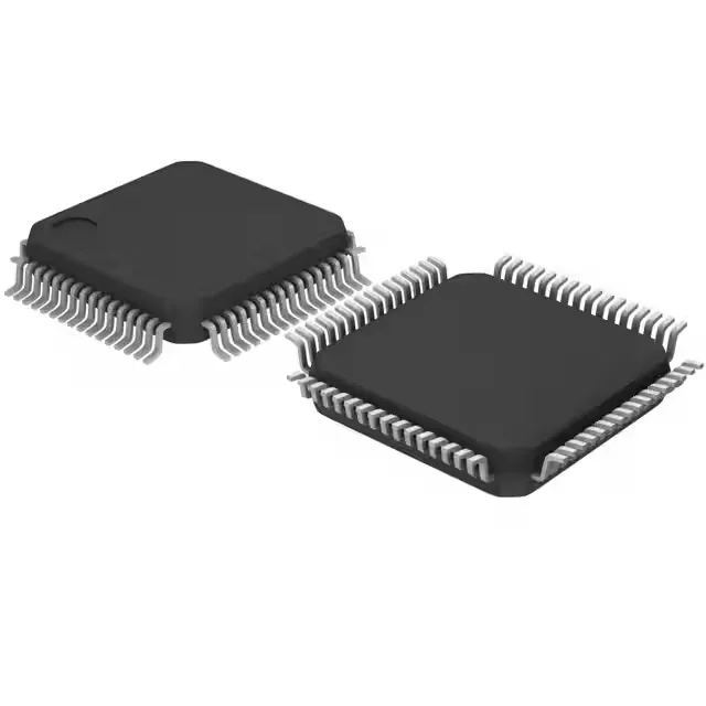
The 51 I/O are distributed around all four sides, so a two-layer PCB is feasible for many designs if the routing is kept clean. The exposed pad (if present on this package variant) should be connected to ground with a thermal via array for best heat transfer.
The STM32F100RDT7B includes DMA, a power-down reset (PDR), power-on reset (POR), programmable voltage detector (PVD), PWM timers, a temperature sensor, and a watchdog timer.