What the 24 MHz Cortex-M3 buys you on a control board
Memory sizing — 256 KB Flash, 24 KB SRAM
256 KB of Flash is the mid-density option in the STM32F100 line — enough for a real-time control stack with a modest communications protocol (Modbus RTU, CANopen) and a bootloader, but tight if you are adding a GUI framebuffer or over-the-air update staging. The 24 KB SRAM splits between stack, heap, and DMA buffers; a firmware engineer should budget the DMA descriptors and ADC result arrays early. If the application needs more than 24 KB of working memory, the next step up in the STM32F1 family doubles the SRAM.
Peripherals and connectivity — what is on the bus
On-chip peripherals include DMA, a power-on reset (POR), a programmable voltage detector (PVD), PWM timers, a temperature sensor, and a watchdog timer.
Package and footprint — 64-LQFP
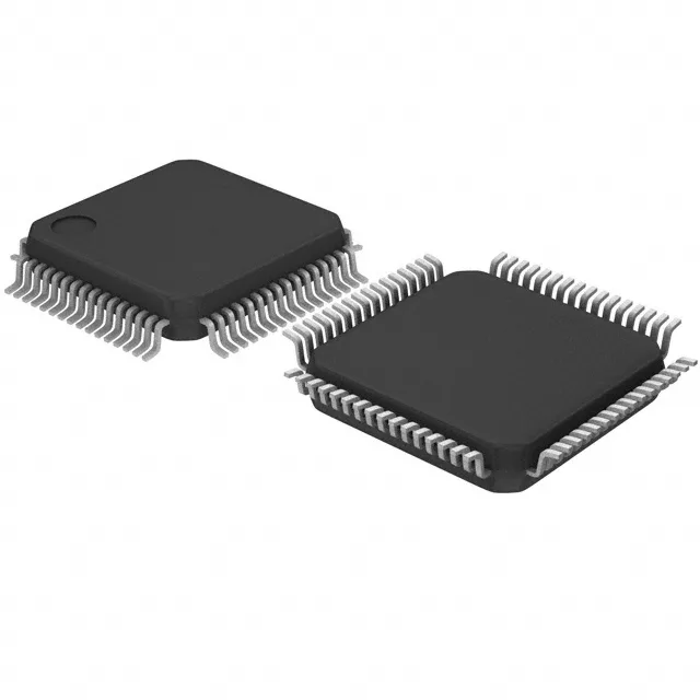
Housed in a 64-LQFP with a 10x10 mm body and 0.5 mm pitch, the STM32F100RCT6B is a hand-solderable surface-mount package — no hot-air station required for a field swap if the board has been designed with accessible pads. The 51 I/O lines are distributed around the four sides; a layout engineer should check the pin assignment against the peripheral multiplexing table before committing the PCB.
STMicroelectronics lists the STM32F100RCT6B as Active. The part is ROHS3 compliant.