Value-line Cortex-M3 in a BGA — what the 64-TFBGA means for your board
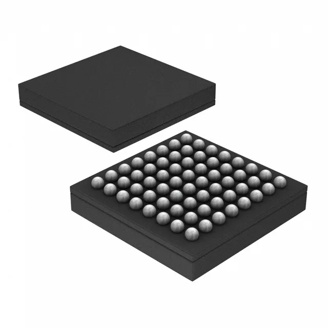
The part is built for cost-sensitive control applications — motor drives, sensor hubs, human-machine interfaces, and industrial I/O nodes — where the 24 MHz core and peripheral set (DMA, PWM, multiple serial interfaces) cover the logic without over-spending on a higher-performance tier. The distinguishing feature here is the package: 64-TFBGA. That is a fine-pitch ball-grid array, not the more common LQFP-64. The BGA saves board area — the balls sit under the body — but it demands a multi-layer PCB with micro-vias or blind vias to route the signals out. If your production line is set up for QFP packages only, this package adds process cost.
24 MHz core and 128 KB Flash — sizing the firmware and throughput budget
The 24 MHz ARM Cortex-M3 core delivers about 30 DMIPS — enough for real-time control loops running at a few kilohertz, Modbus or CAN node processing, and basic sensor fusion. The 128 KB Flash is the hard firmware-size ceiling; a design that compiles to 90 KB today leaves 38 KB for future field updates over UART or SPI. The 8K x 8 SRAM is tight for buffering — a 4 KB DMA buffer for an ADC scan sequence consumes half of it, so memory-conscious coding is required. The integrated 12-bit ADC has 16 channels, and the dual 12-bit DAC covers analog output needs. DMA offloads peripheral transfers from the core. The serial interface set — I²C, SPI, UART/USART, plus IrDA and LIN — covers most industrial and appliance communication requirements.
The internal oscillator and power-on reset (POR/PDR) reduce external BOM count.
STMicroelectronics lists the STM32F100RBH6BTR as Active. For new designs, the entire STM32F100 value line shares the same Cortex-M3 core and peripheral IP, so a pin-compatible migration to a larger Flash or RAM variant within the family is possible without a board respin — as long as the package stays the same.