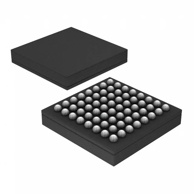
Value-line Cortex-M3 in a BGA — what the 24 MHz and 16 KB Flash mean for your BOM
The STM32F100R4H6B is STMicroelectronics' entry-point STM32F1 value-line MCU built around an ARM Cortex-M3 core running at 24 MHz. The 51 general-purpose I/O pins in a 64-TFBGA package give you more signal routing than a comparable 48-pin QFP, at the cost of a BGA footprint that requires via fanout and X-ray inspection on the line.
Flash and RAM budget — sizing the firmware before you commit
16 KB of program memory (16K x 8) and 4 KB of SRAM (4K x 8) are the hard limits for this part. A bare-metal UART-to-sensor bridge or a simple PWM fan controller fits comfortably. If your application needs a CANopen stack, a USB device stack, or any non-trivial data logging buffer, the memory ceiling will force a move up the STM32F100 density ladder — the 32 KB or 64 KB Flash siblings share the same pinout and peripherals, so the board spin is minimal.
64-TFBGA — layout and rework considerations
The exposed center pad is not a thermal slug — it's a ground-plane tie for signal integrity. For rework, a hot-air profile with bottom-side preheat is standard; expect to X-ray every joint because the balls under the die are not visually inspectable.
Supply range and logic levels
The VDD range is 2.0 V to 3.6 V, so the part runs on a single 3.3 V rail without a regulator. All I/O are 3.3 V tolerant; 5 V-tolerant inputs are not available on this value-line variant, so level shifting is required when interfacing with 5 V peripherals.
On-chip peripherals include DMA, a power-on reset (POR), a programmable voltage detector (PVD), a temperature sensor, and a watchdog timer. The 12-bit ADC has 16 multiplexed channels; the 12-bit DAC has two channels. No USB or CAN peripheral on this die, so those interfaces need an external transceiver or a different STM32F1 variant.
For dual-sourcing resilience, the pin-compatible STM32F100R6H6B (32 KB Flash) and STM32F100R8H6B (64 KB Flash) are direct drop-in alternatives within the same package and temperature grade.