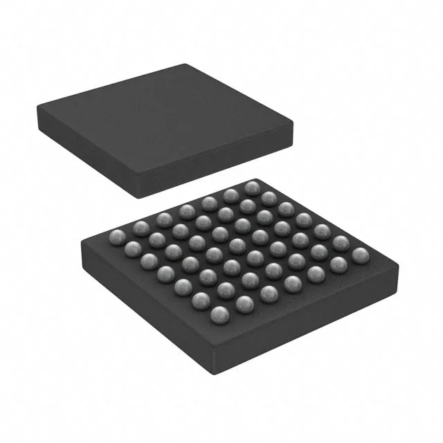
The STM32F072CBY6TR: It packs USB 2.0 full-speed, CANbus, multiple I²C and SPI interfaces, a 12-bit ADC with ten channels, and a dual 12-bit DAC into a 49-ball WLCSP that sits about the size of a grain of rice.
128 KB Flash, 16 KB SRAM — sizing the firmware and buffer budget
The 128 KB program Flash is enough for a USB stack with a custom HID or CDC class, a CANopen node, and a modest application loop. The 16 KB SRAM (organized as 16K x 8) handles a couple of 1 KB DMA buffers plus the stack and heap — if you are doing heavy audio or graphics frame buffering, you will bump the ceiling. The 48 MHz PLL needs one flash wait state above 24 MHz; the hardware prefetch helps keep tight loops running without stalling.
49-WLCSP — board-level reality for the rework bench
No exposed pad to stitch — thermal dissipation goes through the balls into the PCB copper. On the rework bench, hot-air station with a fine nozzle and a preheat plate below the board; do not pry — the die is the package, and the balls shear before the silicon gives.
Peripherals and connectivity — what the 37 I/O give you
With 37 I/O on a 49-ball package, the pinout is dense. The peripheral set includes a DMA controller, I²S audio interface, POR/PWM timers, and a watchdog. The USB peripheral has its own 48 MHz oscillator sourced from the internal PLL — no external crystal needed for USB if the clock trimming is within tolerance. The 10-channel 12-bit ADC samples up to 1 MSps; the two 12-bit DAC channels are useful for analog set-point generation or audio output.
ROHS3 compliant. The base product number is STM32F072, so PCNs and errata are tracked under that family umbrella.