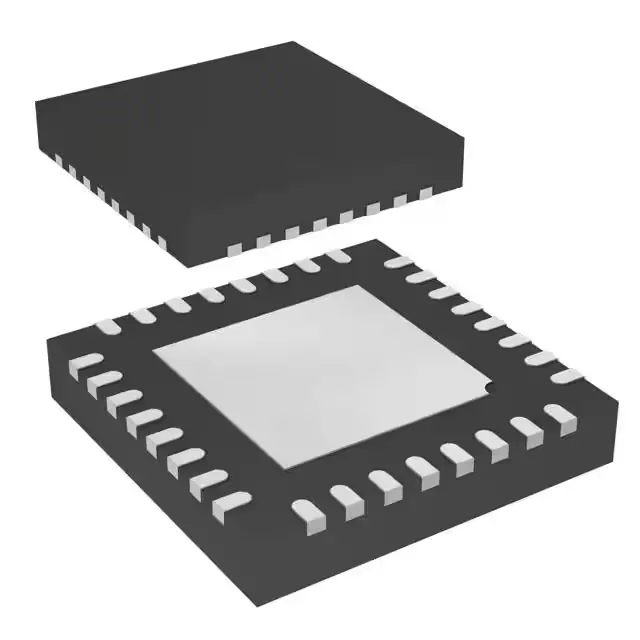
The STM32F051K4U7: The ARM Cortex-M0 core runs at 48 MHz, which is the maximum clock for the STM32F0 value line. At this speed the part can handle a single sensor-fusion loop, a UART-to-SPI bridge, or a simple motor-control PWM cycle without stalling. The 48 MHz PLL requires one flash wait state above 24 MHz — the hardware handles it automatically, but the timing budget for tight ISRs should account for the fetch penalty. The 16 KB program memory suits a single-purpose control algorithm, a bootloader plus a modest application, or a Modbus slave stack. The 8 KB SRAM leaves room for a few hundred bytes of stack and a moderate-size data buffer — enough for a 256-byte UART FIFO and a 2 KB ADC sample array.
Industrial temperature range and the UFQFN footprint
The 105°C upper limit is the extended industrial grade; the part will hold its timing and ADC accuracy across that span, but the internal oscillator drifts more at the extremes, so a crystal is recommended for precision timing. The 32-UFQFN with exposed pad is a space-saving, thermally enhanced package. The pad is the only thermal path — without a via stitch under the package, junction temperature rises quickly above 85°C ambient.
Peripherals and I/O count for the BOM
The 27 I/O lines in this 32-pin package give enough headroom for a 16-bit parallel LCD interface, a keypad matrix, or a handful of sensor interrupts alongside the communication peripherals. The integrated DMA, I²S, POR, PWM, and WDT reduce external component count — no need for a separate watchdog or POR supervisor. The HDMI-CEC block is a niche feature for consumer AV equipment; most industrial designs will leave it unused. The 13-channel 12-bit ADC and single 12-bit DAC cover analog front-end needs for current sensing, temperature monitoring, or set-point generation.