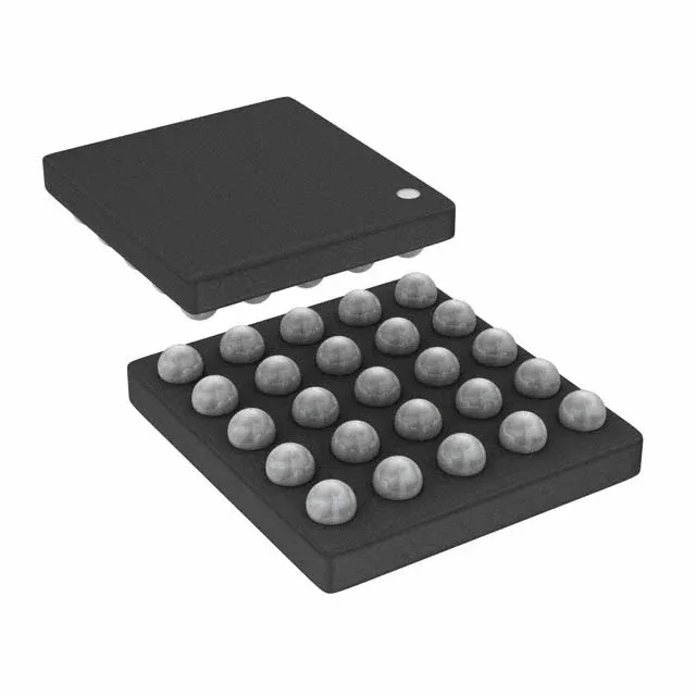
48 MHz Cortex-M0 in a 25-WLCSP — the space-constrained control MCU
The STM32F031E6Y6TR: It targets cost-sensitive, space-constrained embedded control applications — motor commutation, sensor fusion, simple HMI, and I/O expansion — where the 25-WLCSP package saves board area versus a TSSOP or QFN. The 20 available I/O lines and peripheral set including DMA, I²S, POR, PWM, and WDT give it the basic timing and data-movement hardware for a single-loop control task without an external supervisor.
32 KB Flash, 4 KB SRAM — sizing the firmware budget
The 32 KB Flash (32K x 8) and 4 KB SRAM (4K x 8) define the application envelope. This is the entry-density tier of the STM32F0 family, suited for a single firmware image with a modest state machine, a few hundred lines of control logic, and a small data buffer. The 12-bit ADC with 13 channels covers analog sensing — thermistor, current shunt, or potentiometer feedback — without an external converter. Designs that need a USB stack, a larger lookup table, or over-the-air update staging will outgrow this memory budget; the STM32F031 series steps up through 64 KB Flash options in the same WLCSP footprint.
25-WLCSP — what the package means for assembly and procurement
The 25-WLCSP (Wafer-Level Chip-Scale Package) is the smallest physical footprint for this MCU — roughly 2.5 mm × 2.5 mm, with solder balls on a 0.4 mm pitch. That shrinks the PCB real estate to nearly the die size, which matters for wearable, sensor-pod, or multi-layer rigid-flex designs. The trade-off: WLCSP requires a controlled SMT process with stencil design matched to the ball diameter, and rework is difficult without a dedicated BGA rework station.