16 KB Flash — sizing the firmware budget
The 16 KB Flash (16K x 8) is the hard limit for application code and bootloader combined. Typical firmware for a UART-to-I2C bridge, a simple PWM fan controller, or a single-zone temperature monitor fits comfortably. If the project needs a USB stack, a real-time OS kernel, or over-the-air update staging, the Flash budget gets tight — the pin-compatible STM32F031C6T6TR doubles the Flash to 32 KB and is worth evaluating before the layout locks. The 4 KB SRAM (4K x 8) supports moderate data buffers and a few stack frames; DMA offloads peripheral transfers without consuming CPU cycles.
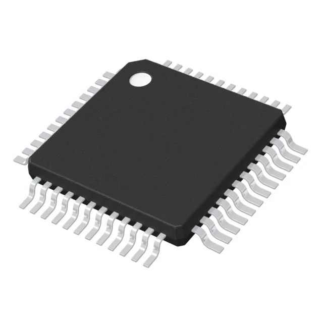
48-LQFP package — footprint and routing
Housed in a 48-LQFP (7x7 mm) with 0.5 mm pitch, the STM32F031C4T6TR uses a standard JEDEC footprint that routes easily on two-layer boards. The 39 I/Os are distributed around all four sides; the supply pins (VDD, VDDA, VSS) sit on opposite corners, so a 100 nF ceramic per supply pair plus a bulk 4.7 µF on the main 3.3 V rail covers decoupling. The exposed pad is not present on this package — thermal dissipation relies on the leadframe and airflow, adequate for the sub-100 mA typical draw at 48 MHz.
The base product number STM32F031 spans multiple Flash and SRAM density variants in the same package, so a firmware-only migration to a higher-density sibling (e.g., STM32F031C6T6TR) is possible without a board spin.
Sourcing posture
As an active STM32 part, the STM32F031C4T6TR is available through the independent distribution channel. For volume production, a firm lead time is quoted per order — no allocation constraints are currently reported on this density tier.