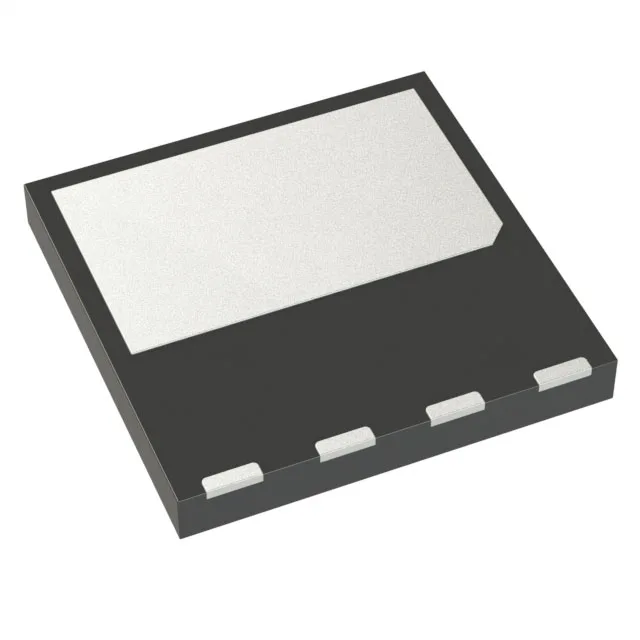
600 V, 25 A switching cell in a PowerFlat HV package
The 44.3 nC typical gate charge at 10 V means the gate-drive power budget is moderate — a 1 A driver can switch this FET in the 100–200 kHz range without excessive dissipation in the driver IC.
On-resistance and gate charge at the operating point
For a 12.5 A load at 100°C junction, budget roughly 1.5× the 25°C value. Input capacitance Ciss is 1960 pF typical at Vds=100 V. That capacitance, combined with the 44.3 nC gate charge, determines the switching transition time and the cross-conduction window during hard-switched transitions.
Active production, ROHS3, wide temperature range
The PowerFlat™ (8x8) HV package is a surface-mount 8-PowerVDFN with an exposed pad for heat sinking through the PCB. The thermal pad area on the board sets the junction-to-ambient thermal resistance — the datasheet layout recommendation is worth following for the full 160 W power dissipation rating.