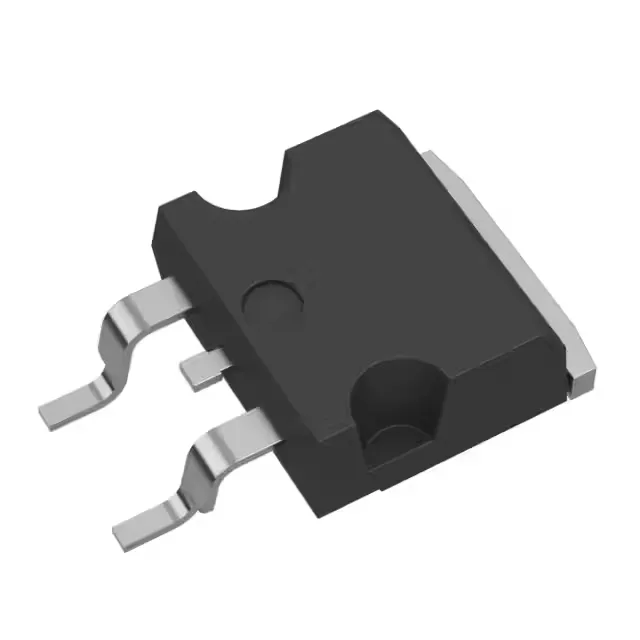
STMicroelectronics STH200N10WF7-2 — Discrete Semiconductors

STH200N10WF7-2 N-Channel MOSFET, 100V, 180A, 4mOhm

MPNSTH200N10WF7-2
End of Life

STMicroelectronics STH200N10WF7-2, N-Channel MOSFET, 100 V Vdss, 180 A continuous drain, 4 mOhm Rds(on) at 90 A / 10 V, TO-263-3 (D2Pak), -55°C to 175°C.

$6.97Ref. price · indicative, final on quote
PackagingTO-263-3, D²Pak (2 Leads + Tab), TO-263AB
RoHSROHS3 Compliant
Independent supplier — new & surplus stockAuthenticity-screened · ESD-safe packingListing updated Aug 2026

Specifications

STH200N10WF7-2 specifications
ParameterValue
FET typeN-Channel
MountingSurface Mount
Drain to source voltage100 V
Drive voltage (Max rds on, min rds on)10V
Current - continuous drain (Id) @ 25°C180A (Tc)
Power dissipation340W (Tc)
Operating temperature-55°C ~ 175°C (TJ)
PackageTape & Reel (TR); Cut Tape (CT)
Vgs±20V
TechnologyMOSFET (Metal Oxide)
CaseTO-263-3, D²Pak (2 Leads + Tab), TO-263AB
Vgs(th) (Max) @ id4.5V @ 250µA
Rds on (Max) @ id, vgs4mOhm @ 90A, 10V
Gate charge (Qg) (Max) @ vgs93 nC @ 10 V
Input capacitance (Ciss) (Max) @ vds4430 pF @ 25 V

Product details

What this MOSFET is built for

The STH200N10WF7-2 is an N-channel power MOSFET in the STripFET F7 family, rated for 100 V drain-source and 180 A continuous drain current. The TO-263-3 (D2Pak) surface-mount package with a large exposed tab lets you pull heat into the board plane; the 340 W power dissipation rating at the case tells you the thermal path is the limiting factor, not the silicon.

Gate drive and switching behaviour

Gate charge is 93 nC at 10 V, and the recommended drive voltage is 10 V for the lowest Rds(on). The 4.5 V threshold at 250 µA means a logic-level gate driver at 5 V will turn the device on, but the Rds(on) will be higher than the 4 mOhm spec — the 10 V drive figure is the one to design to for full conduction. Input capacitance of 4430 pF at 25 V drain-source is moderate for this current class; the gate driver needs to source and sink enough peak current to hit the switching speed the application requires without excessive cross-conduction.

Thermal and environmental reach

The 340 W dissipation at the case is a theoretical ceiling — real-world derating depends on the PCB copper area and airflow. The D2Pak tab is the primary heat path; a thermal-via array under the tab is standard practice for keeping junction temperature inside the 175°C limit at full load.

Frequently asked questions

What is the closest pin-compatible alternative to STH200N10WF7-2?

The STP200N10F7 is a through-hole (TO-220) variant with the same 100 V / 180 A rating and similar Rds(on). The die is the same STripFET F7 generation, but the package differs — the STH200N10WF7-2 is surface-mount D2Pak, while the STP200N10F7 is TO-220. They are not pin-compatible; the footprint and thermal management approach are different.

Does STH200N10WF7-2 require a heatsink?

At 180 A continuous drain, the 4 mOhm Rds(on) still produces over 130 W of conduction loss at full current. The D2Pak tab can sink significant heat into the PCB copper plane, but a dedicated heatsink or forced airflow is typically required to keep the junction below 175°C at high duty cycles.