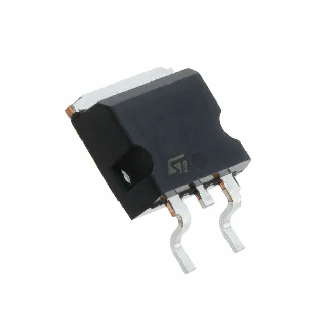
STMicroelectronics STGB10M65DF2

STGB10M65DF2 IGBT, 650 V 20 A Trench Field Stop, D2PAK

MPNSTGB10M65DF2
End of Life

STMicroelectronics STGB10M65DF2 Trench Field Stop IGBT, 650 V Vces, 20 A Ic, 115 W, 28 nC Qg, TO-263-3 (D2PAK), -55 to 175 °C.

$2.16Ref. price · indicative, final on quote
PackagingTO-263-3, D2PAK (2 Leads + Tab), TO-263AB
RoHSROHS3 Compliant
Independent supplier — new & surplus stockAuthenticity-screened · ESD-safe packingListing updated Jul 2026

Specifications

STGB10M65DF2 specifications
ParameterValue
IGBT typeTrench Field Stop
Input typeStandard
MountingSurface Mount
Voltage - collector emitter breakdown650 V
Current - collector (Ic)20 A
Current - collector pulsed40 A
Power - max115 W
Operating temperature-55°C ~ 175°C (TJ)
PackageTape & Reel (TR); Cut Tape (CT)
Gate charge28 nC
CaseTO-263-3, D2PAK (2 Leads + Tab), TO-263AB
Test condition400V, 10A, 22Ohm, 15V
Switching energy120µJ (on), 270µJ (off)
Td (on/off) @ 25°C19ns/91ns
Vce(on) (Max) @ vge, ic2V @ 15V, 10A
Reverse recovery time96 ns

Product details

The STGB10M65DF2 is a 650 V, 20 A Trench Field Stop IGBT from STMicroelectronics, housed in a surface-mount TO-263 (D2PAK) package. The Trench Field Stop structure delivers a low saturation voltage of 2 V at 15 V gate drive and 10 A collector current, combined with fast switching — 19 ns turn-on delay and 91 ns turn-off delay at 25 °C. Typical applications include power factor correction (PFC) stages, motor drives, induction heating, and uninterruptible power supplies (UPS) where the 650 V rating covers 400 V DC bus rails with margin.

Tested at 400 V, 10 A, 22 Ω gate resistor, 15 V gate drive, the STGB10M65DF2 switches 120 µJ on and 270 µJ off. The 28 nC total gate charge means a 1 A gate driver can charge the gate in under 30 ns, keeping switching losses manageable at 20–50 kHz hard-switched frequencies. The 96 ns reverse recovery time (trr) of the internal diode is fast enough for continuous-conduction-mode PFC without external fast-recovery diodes in most designs.

Thermal and package — mounting the D2PAK on the board

The maximum power dissipation is 115 W, but the real junction-to-ambient thermal resistance depends on the PCB copper area — a 2 oz copper pour of at least 6 cm² under the tab is typical for keeping the junction below 175 °C at 10 A continuous.

ROHS3 compliant.

Frequently asked questions

Is the STGB10M65DF2 suitable for high-frequency switching like PFC?

Yes. With 28 nC gate charge and 120 µJ / 270 µJ switching energy at 400 V, 10 A, the STGB10M65DF2 is well-suited for hard-switched PFC stages operating at 20–50 kHz. The fast turn-on/off delays (19 ns / 91 ns) keep dead-time losses low.

What is the difference between STGB10M65DF2 and the older STGB10M60DF2?

The primary difference is the voltage rating: the STGB10M65DF2 is rated at 650 V Vces versus the STGB10M60DF2's 600 V. The 650 V part provides additional margin on 400 V DC bus rails and is the recommended replacement for new designs requiring higher voltage headroom.