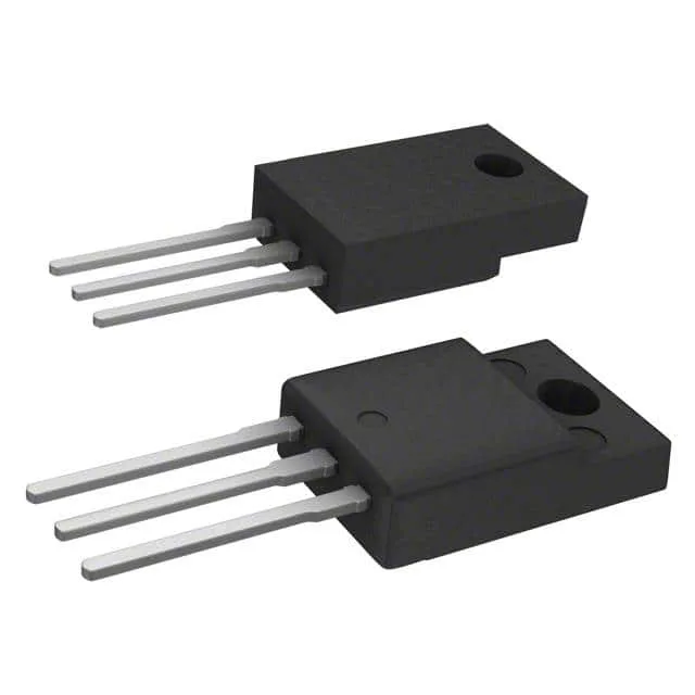
STMicroelectronics STF25NM50N — Discrete Semiconductors

STF25NM50N N-Channel MOSFET, 500 V, 22 A, TO-220FP

MPNSTF25NM50N
Obsolete

STMicroelectronics STF25NM50N, MDmesh™ II series, N-Channel MOSFET, 500 V Vdss, 22 A Id, 140 mOhm Rds(on) at 10 V, TO-220-3 Full Pack, Through Hole, -55°C to 150°C.

Independent supplier — new & surplus stockAuthenticity-screened · ESD-safe packingListing updated Jul 2026

Specifications

STF25NM50N specifications
ParameterValue
SeriesMDmesh™ II
FET typeN-Channel
MountingThrough Hole
Drain to source voltage500 V
Drive voltage (Max rds on, min rds on)10V
Current - continuous drain (Id) @ 25°C22A (Tc)
Power dissipation40W (Tc)
Operating temperature-55°C~150°C(TJ)
PackageTube
Vgs±25V
TechnologyMOSFET (Metal Oxide)
CaseTO-220-3 Full Pack
Vgs(th) (Max) @ id4V @ 250µA
Rds on (Max) @ id, vgs140mOhm @ 11A, 10V
Gate charge (Qg) (Max) @ vgs84 nC @ 10 V
Input capacitance (Ciss) (Max) @ vds2565 pF @ 25 V

Product details

The STF25NM50N: The device is built on ST's MDmesh™ II technology, which reduces on-resistance and gate charge compared to planar MOSFETs of the same voltage class.

140 mOhm on-resistance and 84 nC gate charge — sizing the drive and thermal budget

At 22 A continuous drain, conduction loss (I²R) reaches 68 W at the Rds(on) maximum — exceeding the 40 W package power dissipation limit, so the device must be operated with derating or in pulsed applications where average current stays within the SOA. Input capacitance is 2565 pF at 25 V drain-source, which influences the drive circuit's turn-on delay and the Miller plateau duration.

Frequently asked questions

STF25NM50N vs STF25NM60N — what is the difference?

The STF25NM60N is a 600 V rated device in the same MDmesh™ II family, while the STF25NM50N is rated at 500 V. The 600 V variant offers higher voltage margin for applications with transient spikes, but the 500 V part typically has slightly lower on-resistance for the same die size. Both share the same TO-220 Full Pack package and pinout.