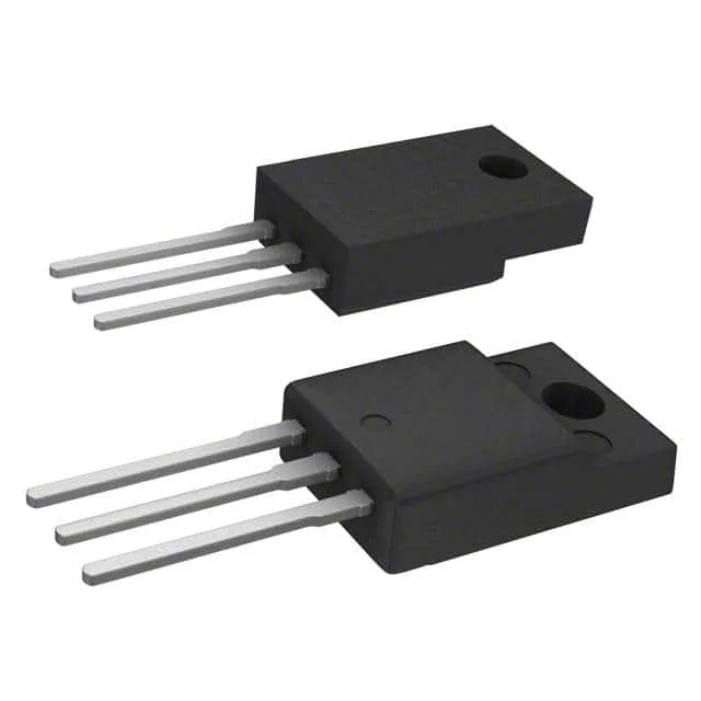
600 V, 18 A N-channel in the isolated TO-220 Full Pack
The STF24N60DM2 is an N-channel power MOSFET from STMicroelectronics' FDmesh™ II Plus series, rated for 600 V drain-source voltage and 18 A continuous drain current at 25°C case temperature. The 200 mOhm max on-resistance at 9 A, 10 V gate drive defines the conduction loss at the operating point — a key number for the thermal budget in a 100 W-class offline flyback or PFC stage. The TO-220 Full Pack (isolated tab) package eliminates the need for a separate insulating pad and washer when bolting to a heatsink — the backside is electrically isolated, so the mounting screw torque and thermal interface material are the only assembly variables. This matters in high-voltage designs where a live tab would require extra creepage clearance.
Gate charge and switching loss — 29 nC at 10 V
Total gate charge Qg is 29 nC at Vgs = 10 V. For a switching frequency of 100 kHz, the average gate drive current required is Qg × fsw = 2.9 mA — well within the capability of a standard gate driver IC. The input capacitance Ciss is 1055 pF at Vds = 100 V; this sets the Miller plateau duration and the turn-on/turn-off delay. The 200 mOhm Rds(on) at 9 A means the conduction loss at 9 A is I²R = 16.2 W, which must be dissipated within the 30 W power dissipation limit at Tc = 25°C. The junction temperature range spans -55°C to 150°C, so the device can handle the thermal cycling of an industrial motor drive or a telecom rectifier that sees ambient swings from cold start to full load. The Vgs(th) maximum is 5 V at 250 µA drain current — the gate threshold is high enough to stay off with a 0 V gate signal even at elevated temperature, which is a standard requirement for a normally-off power switch.