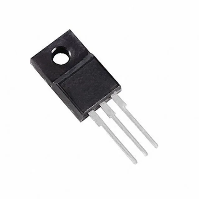
STMicroelectronics STF20NM65N — Discrete Semiconductors

STF20NM65N N-Channel MOSFET, 650 V, 15 A, MDmesh II

MPNSTF20NM65N
Obsolete

STMicroelectronics MDmesh™ II series, N-Channel MOSFET, 650 V drain-source, 15 A continuous drain at 25 °C, 270 mOhm Rds(on) at 10 V drive, 44 nC gate charge, TO-220-3 Full Pack through-hole package, 150 °C junction temperature.

$3.4200Ref. price · indicative, final on quote
Independent supplier — new & surplus stockAuthenticity-screened · ESD-safe packingListing updated Jul 2026

Specifications

STF20NM65N specifications
ParameterValue
SeriesMDmesh™ II
FET typeN-Channel
MountingThrough Hole
Drain to source voltage650 V
Drive voltage (Max rds on, min rds on)10V
Current - continuous drain (Id) @ 25°C15A (Tc)
Power dissipation30W (Tc)
Operating temperature150°C (TJ)
PackageTube
Vgs±25V
TechnologyMOSFET (Metal Oxide)
CaseTO-220-3 Full Pack
Vgs(th) (Max) @ id4V @ 250µA
Rds on (Max) @ id, vgs270mOhm @ 7.5A, 10V
Gate charge (Qg) (Max) @ vgs44 nC @ 10 V
Input capacitance (Ciss) (Max) @ vds1280 pF @ 50 V

Product details

650 V, 15 A N-channel MDmesh™ II in TO-220FP

The STF20NM65N is a 650 V drain-source, 15 A continuous drain N-channel power MOSFET from STMicroelectronics' MDmesh™ II series. The MDmesh™ II technology reduces on-resistance and gate charge compared to planar MOSFETs of the same voltage class. Gate charge totals 44 nC at 10 V gate-source, which keeps switching losses manageable in hard-switched topologies up to the 100 kHz range. Input capacitance measures 1280 pF at 50 V drain-source bias. This saves assembly time and improves thermal interface reliability. Maximum power dissipation is 30 W at case temperature. Junction temperature rating is 150 °C maximum.

The 650 V drain-source voltage gives headroom for 400 V DC bus rails in power factor correction stages or flyback converters, with derating margin for switching transients. The 15 A continuous rating at 25 °C case temperature derates with case heating; at elevated case temperatures the usable current drops per the datasheet curve. At 270 mOhm maximum on-resistance, conduction loss at 7.5 A is roughly 15 W. For lower-duty or lower-current applications the 270 mOhm figure directly scales the I²R loss. Gate charge of 44 nC at 10 V means a 1 A gate driver charges the gate in about 44 ns, which is fast enough for 100 kHz hard-switching without excessive cross-conduction. Slower gate drive or higher switching frequency may increase switching losses.

Frequently asked questions

What is the replacement for STF20NM65N?

No official replacement part number is listed by STMicroelectronics for this obsolete device. A functionally similar current-production N-channel MOSFET in the same voltage and current class may be found within the MDmesh™ series, but pin compatibility and electrical fit must be verified against the design requirements. Submit an RFQ for cross-reference assistance.