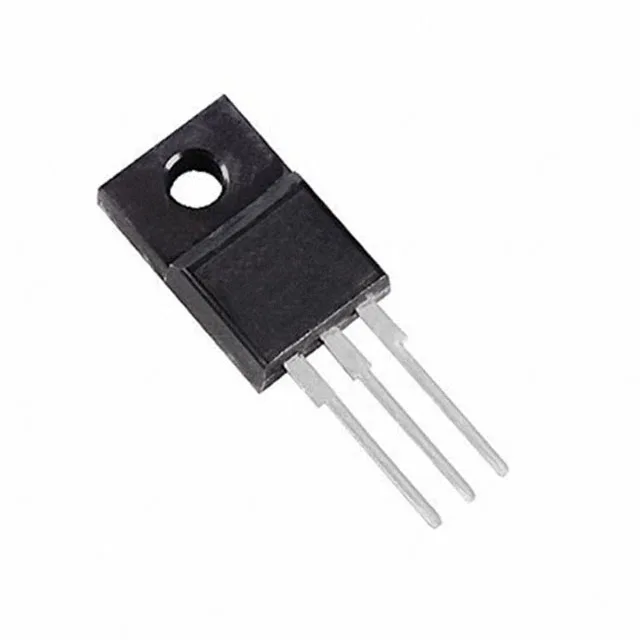
STMicroelectronics STF19NM50N — Discrete Semiconductors

STF19NM50N N-Channel MOSFET, 500V, 14A, TO-220FP

MPNSTF19NM50N
Active

STMicroelectronics MDmesh™ II STF19NM50N, N-Channel MOSFET, 500 V Vdss, 14 A Id, 250 mOhm Rds(on) at 10 V, 34 nC Qg, TO-220-3 Full Pack (TO-220FP), Through Hole, 150°C TJ.

$4.3900Ref. price · indicative, final on quote
PackagingTO-220-3 Full Pack
RoHSROHS3 Compliant
SeriesMDmesh™ II
Independent supplier — new & surplus stockAuthenticity-screened · ESD-safe packingListing updated Aug 2026

Specifications

STF19NM50N specifications
ParameterValue
SeriesMDmesh™ II
FET typeN-Channel
MountingThrough Hole
Drain to source voltage500 V
Drive voltage (Max rds on, min rds on)10V
Current - continuous drain (Id) @ 25°C14A (Tc)
Power dissipation30W (Tc)
Operating temperature150°C (TJ)
PackageTube
Vgs±25V
TechnologyMOSFET (Metal Oxide)
CaseTO-220-3 Full Pack
Vgs(th) (Max) @ id4V @ 250µA
Rds on (Max) @ id, vgs250mOhm @ 7A, 10V
Gate charge (Qg) (Max) @ vgs34 nC @ 10 V
Input capacitance (Ciss) (Max) @ vds1000 pF @ 50 V

Product details

500 V MDmesh™ II switch in an isolated TO-220FP

Conduction and switching parametrics

Rds(on) is specified at 250 mOhm maximum with Vgs = 10 V and Id = 7 A — this is the conduction loss figure the thermal design must budget for at the operating current. The 34 nC total gate charge at 10 V is moderate for a 500 V / 14 A device; a gate driver delivering 1 A can switch the FET in roughly 34 ns, keeping crossover losses manageable in the 50–150 kHz range typical of hard-switched converters. Input capacitance Ciss is 1000 pF at Vds = 50 V, which sets the gate-drive impedance requirement for clean edges without ringing.

The TO-220FP (TO-220 Full Pack) has a fully moulded plastic body with no exposed metal tab — the back of the package is the heatsink face, electrically isolated. Maximum power dissipation is 30 W at case temperature, limited by the junction-to-case thermal resistance of the full-pack construction. For a typical 100 W PFC stage running at 70°C ambient, the designer should verify the junction temperature stays below the 150°C TJ rating.

Frequently asked questions

What is the Rds(on) of STF19NM50N at 10V?

The maximum Rds(on) is 250 mOhm at Vgs = 10 V and Id = 7 A. This is the on-resistance value used for conduction loss calculations in the thermal design.

Can STF19NM50N be used for switching power supplies?

Yes — the 500 V Vdss, 14 A Id, 250 mOhm Rds(on), and 34 nC gate charge make it well suited for hard-switched topologies such as PFC boost stages, flyback converters, and two-switch forward converters in the 50–150 kHz range.