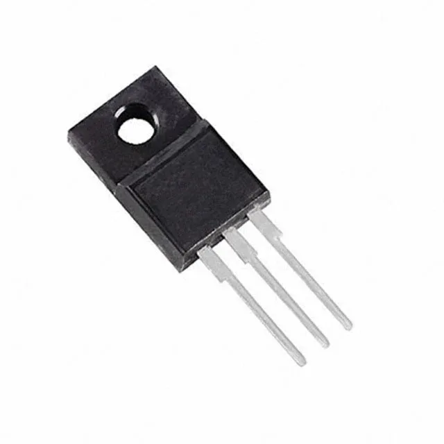
STMicroelectronics STF18NM80 — Discrete Semiconductors

STF18NM80 N-Channel MOSFET, 800 V, 17 A, TO-220FP

MPNSTF18NM80
Active

STMicroelectronics STF18NM80, N-Channel MDmesh™ MOSFET, 800 V Vdss, 17 A Id, 295 mOhm Rds(on) at 10 V, 70 nC Qg, TO-220FP through-hole, 150°C junction.

$7.5300Ref. price · indicative, final on quote
Independent supplier — new & surplus stockAuthenticity-screened · ESD-safe packingListing updated Aug 2026

Specifications

STF18NM80 specifications
ParameterValue
SeriesMDmesh™
FET typeN-Channel
MountingThrough Hole
Drain to source voltage800 V
Drive voltage (Max rds on, min rds on)10V
Current - continuous drain (Id) @ 25°C17A (Tc)
Power dissipation40W (Tc)
Operating temperature150°C(TJ)
PackageTube
Vgs±30V
TechnologyMOSFET (Metal Oxide)
CaseTO-220-3 Full Pack
Vgs(th) (Max) @ id5V @ 250µA
Rds on (Max) @ id, vgs295mOhm @ 8.5A, 10V
Gate charge (Qg) (Max) @ vgs70 nC @ 10 V
Input capacitance (Ciss) (Max) @ vds2070 pF @ 50 V

Product details

800 V MDmesh™ — what this part does in a supply

Gate charge of 70 nC at 10 V is moderate for an 800 V device, meaning a standard gate-driver IC can switch it without excessive drive losses.

Package and mounting — TO-220 Full Pack

The through-hole leads suit point-to-point wiring or PCB mounting with a standard TO-220 footprint. Maximum power dissipation is 40 W at case temperature, which sets the practical limit for continuous operation; the designer should derate based on the actual junction temperature, rated for 150°C maximum.

Frequently asked questions

What is the Rds(on) of the STF18NM80 at 10 V?

This is the figure to use for worst-case conduction loss calculations in the power stage.

Is the STF18NM80 RoHS compliant?

RoHS compliance is standard for current-production STMicroelectronics MDmesh™ MOSFETs, including the STF18NM80. The datasheet and packaging mark confirm lead-free construction.

What is the maximum operating junction temperature of the STF18NM80?

The maximum junction temperature is 150°C. This is the absolute limit for the silicon die; the designer should derate the 40 W power dissipation to keep junction temperature below this value under worst-case ambient conditions.