650 V, 12 A MDmesh V — conduction-loss optimised for offline power
The STF16N65M5 is an N-channel power MOSFET from ST's MDmesh™ V series, rated for 650 V drain-source breakdown and 12 A continuous drain current at 25°C case temperature. The 299 mOhm maximum on-resistance at 6 A, 10 V gate drive is the headline figure for conduction-loss budgeting in a 650 V class part — lower than the M2-generation peers at the same voltage rating, which makes this device a fit where the switching frequency is moderate and the dominant loss is I²R.
Gate charge and switching-speed trade-off
Total gate charge Qg is 45 nC at 10 V gate drive — roughly 2.3× that of the M2-generation STF16N65M2 (19.5 nC). The M5 series achieves lower Rds(on) by using a thicker epitaxial layer, which stores more charge in the drift region; the buyer's trade-off is higher gate-drive current at the target switching frequency. For a 100 kHz hard-switched PFC stage, the average gate current is 4.5 mA (45 nC × 100 kHz), well within a typical driver's capability, but the switching loss per cycle is proportionally higher. Input capacitance Ciss is 1250 pF at 100 V drain-source — a moderate figure for the voltage class. The Miller plateau charge is not separately listed, but the Qgd / Qgs ratio typical of MDmesh V devices keeps the turn-on delay within a few tens of nanoseconds when driven from a standard 10 V gate signal.
TO-220FP — isolated tab, no washer needed
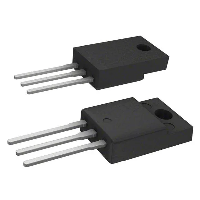
The TO-220 Full Pack (TO-220FP) package has the die mounted on a fully moulded plastic tab — the backside metal is not electrically connected to the drain. This eliminates the need for a silicone pad or mica washer when bolting the device to a heatsink, simplifying assembly and reducing thermal interface resistance. The penalty is a higher junction-to-case thermal resistance than a standard TO-220; the rated power dissipation is 25 W at case temperature, so the thermal budget must account for the full-pack derating.
Active lifecycle and sourcing posture
The STF16N65M5 carries an active lifecycle status — no NRND or EOL flags from STMicroelectronics. ROHS3 compliant per the evidence. Sourced to order against BOM quantities through independent distribution; availability and current pricing confirmed at RFQ.