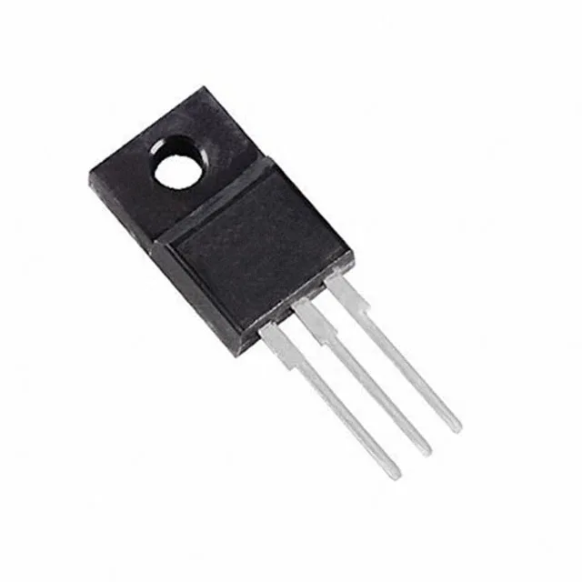
600 V N-channel MOSFET with the MDmesh™ II Plus trench structure
The STF13N60M2: The 17 nC total gate charge keeps the driver current modest.
The 380 mOhm max at 5.5 A, 10 V is the worst-case conduction loss anchor. Input capacitance is 580 pF at 100 V drain-source — that capacitance charges from the driver during the Miller plateau. The low Ciss keeps the turn-on delay short, but the real switching loss depends on the gate resistor and the driver's sink current. The ±25 V maximum gate rating gives margin for ringing on long gate traces, but keep the drive at 10 V to hit the rated Rds(on).
Package reality — TO-220FP full-pack
That saves assembly time and eliminates the thermal interface from the isolation path. The trade-off is higher junction-to-case thermal resistance than a standard TO-220; the 25 W dissipation limit reflects that. Mount it with a clip or screw through the mounting hole, and apply thermal compound between the plastic back and the heatsink surface. Through-hole mounting means the leads carry the mechanical load.
Lifecycle and compliance — current production, no end-of-life shadow
The series is MDmesh™ II Plus, which is ST's mainstream high-voltage MOSFET platform; no successor has been announced for this die and package combination.