Active production — what it means for the BOM line
The STF11NM60ND: ROHS3 compliant — no lead or restricted-substance exemptions to track across date-code lots.
600 V, 10 A, 450 mOhm — sizing the conduction and switching loss
Rated 600 V drain-to-source (Vdss) and 10 A continuous drain current at 25°C case temperature — this sets the bus-voltage ceiling for offline flyback, PFC boost, or bridge topologies and the load current budget before the junction-temperature derating curve applies. Maximum on-resistance is 450 mOhm at 5 A drain current with 10 V gate drive — the conduction loss at full load is I² × R, so at 5 A the dissipation is about 11.25 W, well within the 25 W package limit at 25°C case. Gate charge totals 30 nC at 10 V, and input capacitance is 850 pF at 50 V drain — these numbers drive the gate-driver sizing: a driver sourcing 1 A charges the gate in roughly 30 ns, but the practical switching speed is also limited by the 850 pF input capacitance and the gate-loop inductance.
TO-220 Full Pack — isolated tab, no heatsink pad needed
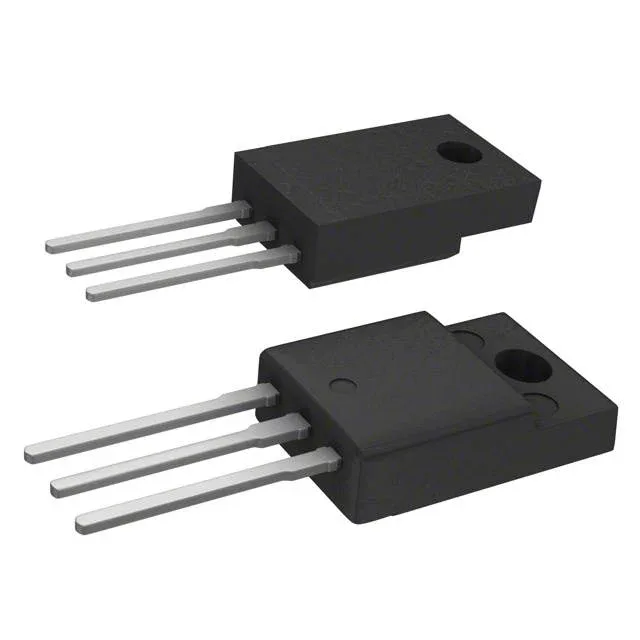
The TO-220 Full Pack (TO-220FP) package has the metal tab fully encapsulated in epoxy — the tab is electrically isolated, so no insulating pad or mica washer is needed between the device and the heatsink, though the thermal resistance junction-to-case is higher than a standard TO-220. Through-hole mounting suits point-to-point wiring or PCB layouts where the 2.54 mm pitch lead frame is standard — the three leads are gate, drain, and source, with the drain on the centre pin. Junction temperature range spans -55°C to 150°C, covering industrial motor-drive environments and some under-hood automotive applications where the ambient stays below 125°C.
FDmesh™ II — fast-recovery body diode for bridge topologies
The FDmesh™ II series integrates a fast-recovery body diode — this reduces reverse-recovery charge (Qrr) compared to a standard MOSFET body diode, making it suited for half-bridge, full-bridge, and LLC resonant converters where the diode conducts during dead-time. Gate threshold voltage is 5 V maximum at 250 µA drain current — the 10 V drive voltage for minimum Rds(on) is well above the threshold, ensuring full enhancement across the operating temperature range.