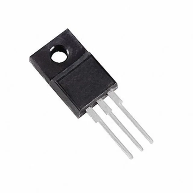
650 V, 7 A — where this MOSFET fits
A total gate charge of 12.5 nC at 10 V is low for a 650 V device in this current class, which means the gate driver does not need to supply much energy per switching cycle. This directly reduces driver losses and allows faster turn-on and turn-off transitions — useful when pushing for efficiency in hard-switched topologies like active clamp flyback or two-switch forward converters. The input capacitance of 410 pF at 100 V Vds is also modest, keeping the Miller plateau short and the switching losses contained.
The trade-off is higher thermal resistance than a standard TO-220; the 25 W power dissipation limit reflects that. Through-hole mounting suits point-of-load assemblies where mechanical robustness matters.