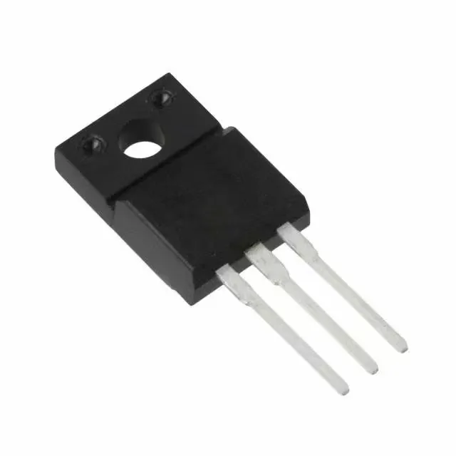
100V, 45A N-channel in a full-pack TO-220
The STF100N10F7 is an N-channel MOSFET from STMicroelectronics' DeepGATE™ and STripFET™ VII series, rated for 100 V drain-to-source voltage and 45 A continuous drain current at 25°C case temperature. The 8 mOhm maximum on-resistance at 22.5 A and 10 V gate drive sets the conduction loss floor — at 45 A the I²R loss is about 16 W, which the 30 W maximum dissipation budget must cover with adequate heatsinking. The TO-220FP full-pack package isolates the tab electrically, so the MOSFET can be bolted directly to a grounded heatsink without an insulating pad — a practical advantage in high-side switching or multi-device layouts where parasitic capacitance to ground matters.
Gate drive and switching budget
Total gate charge is 61 nC at 10 V — a 1 A gate driver charges the gate in about 61 ns, but the 4369 pF input capacitance at 50 V drain bias means the Miller plateau stretches the switching interval; the effective switching loss depends on the driver's peak current and the gate loop inductance. The gate threshold voltage is 4.5 V maximum at 250 µA drain current, and the recommended drive voltage for minimum Rds(on) is 10 V — a 5 V logic-level gate drive will not fully enhance the channel, so a 10 V rail or a dedicated gate driver is needed for rated performance. Maximum gate-to-source voltage is ±20 V — the gate oxide breakdown margin is tight if the driver overshoots; a series gate resistor or a 15 V Zener clamp between gate and source protects against ringing in a hard-switched converter.
Thermal limits and operating range
The junction temperature range spans -55°C to 175°C, covering industrial and automotive under-hood environments — the 175°C absolute maximum allows headroom for transient overloads, but continuous operation above 150°C accelerates electromigration in the aluminum metallization. Maximum power dissipation is 30 W at case temperature 25°C — the TO-220FP's junction-to-case thermal resistance is about 5°C/W, so a 30 W load raises the junction 150°C above the case; a heatsink with 3°C/W or better keeps the junction below 175°C at full rated current.