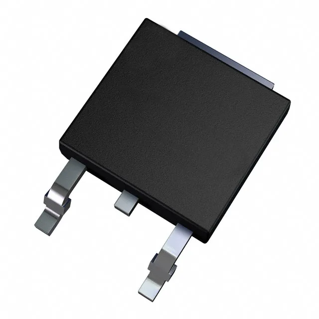
The 500 V rating places it squarely in offline flyback converters, auxiliary power supplies, and 2-switch forward topologies where the primary-side MOSFET sees the rectified mains plus reflected voltage — typically 400 V to 500 V peak on a 230 VAC input with a 1.3× derating margin. At 2.5 A continuous, expect I²R loss of about 4.9 W — well within the 45 W power dissipation capability of the DPAK package when the PCB copper area under the tab is sized correctly.
A typical gate driver sourcing 1 A peak can switch this MOSFET in about 14 ns — fast enough for 100 kHz hard-switching without excessive Miller plateau dwell. The low Qg also means a simple bootstrap supply on the high-side driver is sufficient; no external charge pump or isolated bias rail required. Input capacitance Ciss is 570 pF at 50 V drain bias. Combined with the 14 nC Qg, the switching energy per cycle is modest — the MOSFET is a good fit for medium-frequency converters where the driver IC is a standard 1 A to 2 A part rather than a specialised high-current module.
For volume production commitments, the active lifecycle means no forced redesign cycle from a looming EOL.