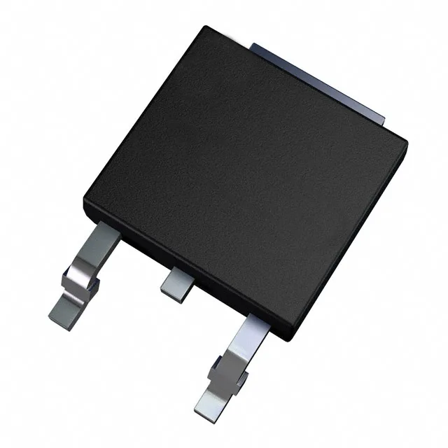
STMicroelectronics STD9N60M2 — Discrete Semiconductors

STD9N60M2 MOSFET N-CH 600V 5.5A DPAK, 780 mOhm Rds(on)

MPNSTD9N60M2
Active

STMicroelectronics MDmesh™ II Plus, STD9N60M2, N-Channel MOSFET, 600 V Vdss, 5.5 A Id, 780 mOhm Rds(on) at 10 V, 10 nC Qg, DPAK (TO-252), Surface Mount, 150 °C TJ.

$1.4100Ref. price · indicative, final on quote
PackagingTO-252-3, DPak (2 Leads + Tab), SC-63
RoHSROHS3 Compliant
SeriesMDmesh™ II Plus
Independent supplier — new & surplus stockAuthenticity-screened · ESD-safe packingListing updated Aug 2026

Specifications

STD9N60M2 specifications
ParameterValue
SeriesMDmesh™ II Plus
FET typeN-Channel
MountingSurface Mount
Drain to source voltage600 V
Drive voltage (Max rds on, min rds on)10V
Current - continuous drain (Id) @ 25°C5.5A (Tc)
Power dissipation60W (Tc)
Operating temperature150°C(TJ)
PackageTape & Reel (TR); Cut Tape (CT)
Vgs±25V
TechnologyMOSFET (Metal Oxide)
CaseTO-252-3, DPak (2 Leads + Tab), SC-63
Vgs(th) (Max) @ id4V @ 250µA
Rds on (Max) @ id, vgs780mOhm @ 3A, 10V
Gate charge (Qg) (Max) @ vgs10 nC @ 10 V
Input capacitance (Ciss) (Max) @ vds320 pF @ 100 V

Product details

600 V N-channel in a DPAK — where the MDmesh™ II Plus fits

This is a 600 V class part, so it is aimed at offline power conversion: flyback converters for AC-DC adapters and chargers, PFC boost stages, auxiliary power supplies in industrial and telecom gear, and LED lighting drivers.

780 mOhm Rds(on) — the conduction loss anchor

That is the number to use for worst-case conduction loss calculations at 25 °C junction — expect it to roughly double at 125 °C junction, which is the normal operating point in a power supply. A 1-inch-square pad on a 2-oz copper board can dissipate roughly 2-3 W before the junction hits 100 °C — that translates to about 1.6 A continuous at 780 mOhm. For higher currents, a heatsink on the tab or forced airflow is needed.

10 nC gate charge — light load on the driver

This means the gate driver only needs to source and sink about 10 nC per switching cycle. The low Qg also keeps the Miller plateau short, reducing the switching loss during the voltage-rise and current-fall overlap. Input capacitance is 320 pF at 100 V drain-source bias. That capacitance charges and discharges through the gate resistor and driver output impedance, setting the turn-on and turn-off delay times. For a typical 10-ohm gate resistor, the RC time constant is about 3.2 ns — fast enough for switching frequencies up to several hundred kilohertz without excessive ringing, provided the PCB layout keeps the gate loop tight.

The base product number is STD9N60, which covers a family of variants in different packages and tape/reel options. The M2 suffix identifies this as the MDmesh™ II Plus generation, offering improved switching performance and lower Rds(on) compared to the earlier MDmesh™ generation.

Frequently asked questions

What is the Rds(on) of STD9N60M2?

The maximum Rds(on) is 780 mOhm at a drain current of 3 A and a gate-source voltage of 10 V. This is the worst-case value at 25 °C junction temperature; the typical on-resistance is lower, and it increases with temperature.

What is the closest pin-compatible alternative to STD9N60M2 in this component family?

Within the MDmesh™ II Plus family, the STD9N60M2 is the 600 V, 5.5 A, 780 mOhm variant in DPAK. Higher-current siblings in the same package and voltage class include the STD11N60M2 (11 A, 450 mOhm) and the STD7N60M2 (7 A, 1.1 ohm). All share the same DPAK footprint and gate drive requirements, so a BOM swap is possible if the current and Rds(on) budget allow.