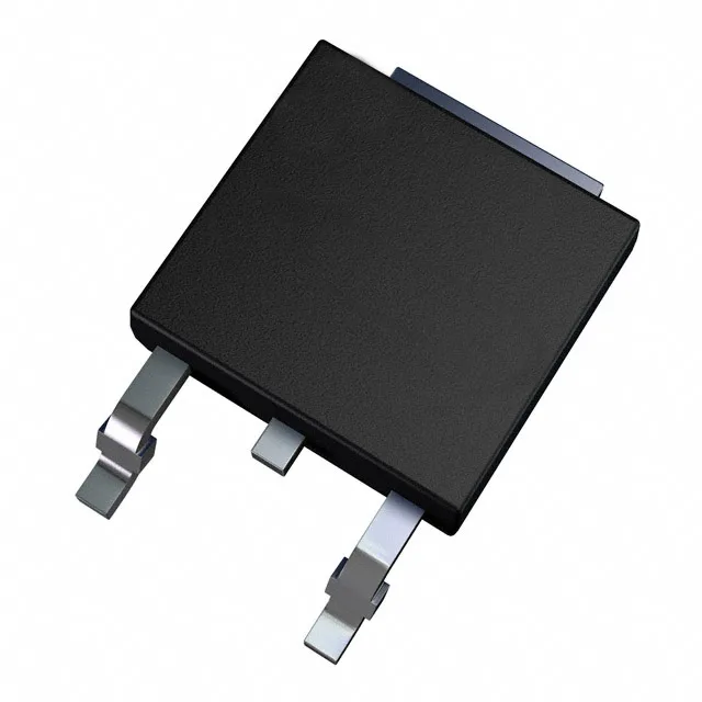
400 V N-channel switch in DPAK
The STD7NK40ZT4 is an N-channel enhancement-mode MOSFET from ST's SuperMESH™ series, housed in a DPAK (TO-252) surface-mount package. It is specified for 400 V drain-source breakdown and 5.4 A continuous drain current at 25 °C case temperature. With a maximum Rds(on) of 1 Ω at Vgs = 10 V and Id = 2.7 A, the on-resistance at the operating junction temperature will be higher — the 25 °C figure is the starting point for loss budgeting, not the in-circuit value.
Gate drive and switching loss budget
Total gate charge is 26 nC at Vgs = 10 V — the drive current required to switch at a given frequency is Qg × fsw. A 100 kHz switching rate draws 2.6 mA from the gate driver, well within the capability of a standard MOSFET driver IC. Input capacitance Ciss is 535 pF at Vds = 25 V, which sets the Miller plateau duration during switching transitions. The 10 V drive voltage is the recommended gate bias for minimum on-resistance; the threshold is 4.5 V max at 50 µA drain current, so a 5 V logic-level gate signal may not fully enhance the channel. Maximum gate-source voltage is ±30 V — a standard 12 V or 15 V gate drive is safe, but a series resistor is advisable if the driver supply can overshoot beyond the abs-max rating during fast turn-off.
Thermal envelope and package integration
The DPAK (TO-252) footprint with the exposed drain tab requires a copper pad on the PCB for heat sinking. The maximum power dissipation is 70 W at case temperature — the actual continuous dissipation is derated by the junction-to-ambient thermal resistance of the board layout, typically 50–80 °C/W on a 1 oz copper pour. Operating junction temperature range is -55 °C to +150 °C, which covers industrial and automotive under-hood environments. The 150 °C ceiling is the absolute limit; reliability degrades above 125 °C continuous, so a 20 % derating on power dissipation is standard practice for a 125 °C max junction design.
Active lifecycle and sourcing posture
The part is available through independent distribution channels. Sourcing is quoted to order against the BOM line — availability and current pricing are confirmed at RFQ time, with no stock-holding claim on this listing.