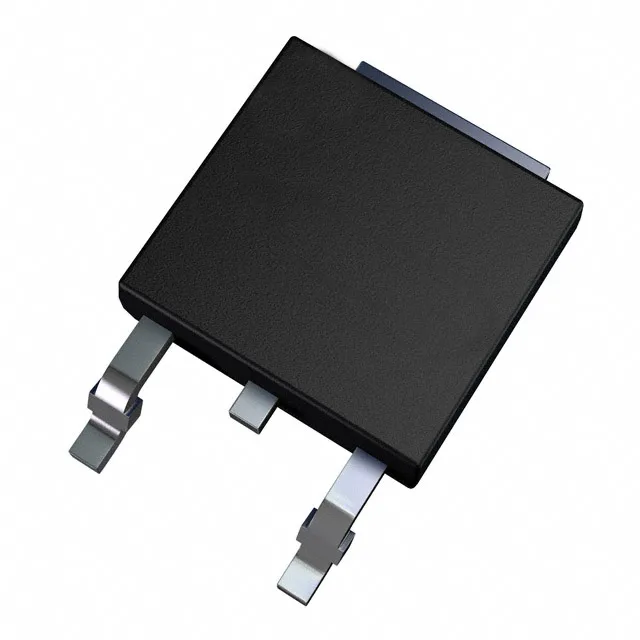
Active high-voltage N-channel MOSFET in DPAK
It is built on a strip-layout vertical DMOS process that delivers low on-resistance and fast switching for offline power supplies, LED lighting drivers, and auxiliary converters in industrial and consumer equipment.
The 10 V drive voltage is typical for standard gate-drive ICs in offline converters; the threshold voltage maxes at 4.5 V at 50 µA, so a logic-level gate signal (5 V) will not fully enhance the channel — plan for a 10 V bias rail or a bootstrap supply.
These numbers indicate moderate switching losses for a 525 V device — suitable for hard-switched topologies up to 100 kHz or so, but not optimised for the lowest gate-drive power in very high frequency designs. The 34 nC Qg means a typical gate-driver with 1 A peak current can charge the gate in about 34 ns, though practical turn-on/off times depend on the external gate resistor and the Miller plateau.
The STD7N52K3 is supplied in the TO-252-3 (DPAK) surface-mount package, a common footprint for medium-power MOSFETs. Maximum power dissipation is 90 W at case temperature, but the real limit is set by the junction temperature ceiling of 150°C.
No official second-source cross-reference is listed, but the base part STD7N52 covers the same die in other package variants if a different footprint is acceptable.