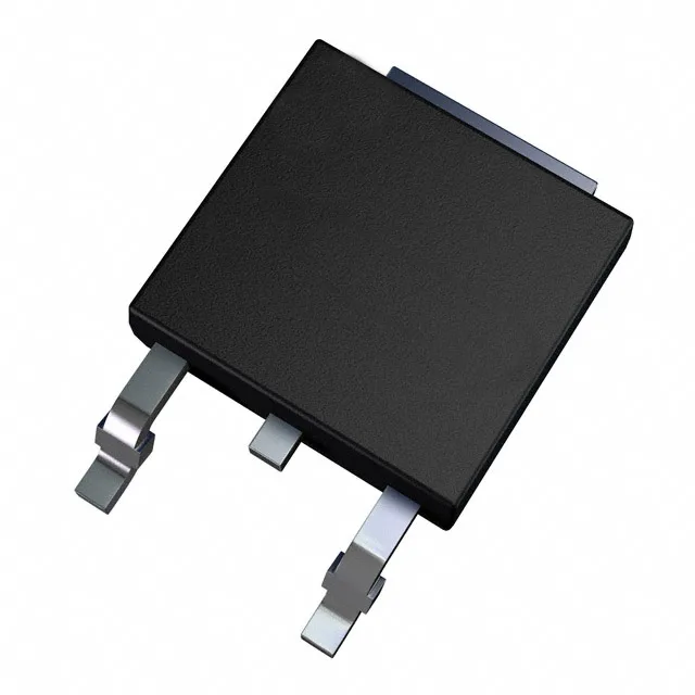
500 V / 3 A N-channel MOSFET — SuperMESH™ series
On-resistance, gate charge, and switching performance
Maximum on-resistance is 2.7 Ohm at a drain current of 1.5 A with 10 V gate drive — this is the conduction loss figure for the power stage. The gate drive voltage is specified at 10 V for the rated Rds(on); a lower gate voltage will increase the on-resistance. Input capacitance Ciss is 310 pF at 25 V drain-source, consistent with the modest die size.
Thermal and environmental ratings
Maximum power dissipation is 45 W at the case temperature. Gate-source voltage is clamped at ±30 V maximum — a common zener-protected input that tolerates transient spikes on the gate drive line.
Package: DPAK (TO-252) surface-mount
The DPAK footprint is a standard power-package layout; the reeled format is Tape & Reel.
Lifecycle and sourcing — NRND status
For a BOM line already using this device, sourcing is available against an RFQ through the surplus and broker channel. Buyers evaluating new designs should select an active N-channel MOSFET with equivalent 500 V / 3 A ratings and a DPAK footprint.