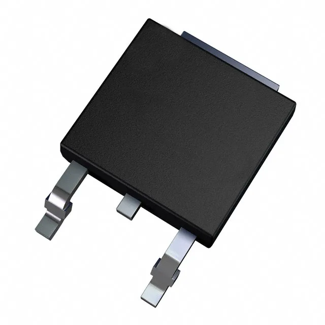
800 V breakdown in a DPAK — sizing the primary switch
At 3 A continuous current, expect roughly 23 W dissipation in the channel before the package thermal resistance is factored in — the 60 W package limit at case temperature gives a healthy derating margin for typical 10–20 W designs.
Gate charge and input capacitance — driver budget
Total gate charge is 3.7 nC at 10 V, and input capacitance is 122 pF at 100 V drain bias. A standard PWM controller with a 1 A peak gate drive can switch this MOSFET at 100 kHz without a separate driver IC.
Temperature range — where it survives
It is ROHS3 compliant.