The 60 V drain-source rating (Vdss) gives headroom for clamping inductive loads in motor drives and DC-DC converters without avalanche stress at nominal bus voltage.
Gate drive and switching — the 5 V / 10 V drive voltage split
The drive voltage range is specified at 5 V and 10 V for the Rds(on) max condition, which tells you this part is not a logic-level MOSFET — it needs a gate drive above the threshold (2.5 V max at 250 µA) to achieve the rated on-resistance. At 5 V gate drive expect higher conduction loss than the 28 mOhm figure; the 10 V drive is the condition for the headline Rds(on). The gate charge is 41 nC at 5 V, which is moderate for a 30 A device — a gate driver with 1 A peak current can switch it in the tens of nanoseconds, but the 2370 pF input capacitance at 25 V drain-source means the driver's source/sink impedance sets the actual turn-on and turn-off times. For hard-switched applications above 50 kHz, factor the gate-drive losses into the thermal budget.
DPAK footprint — board-level fit
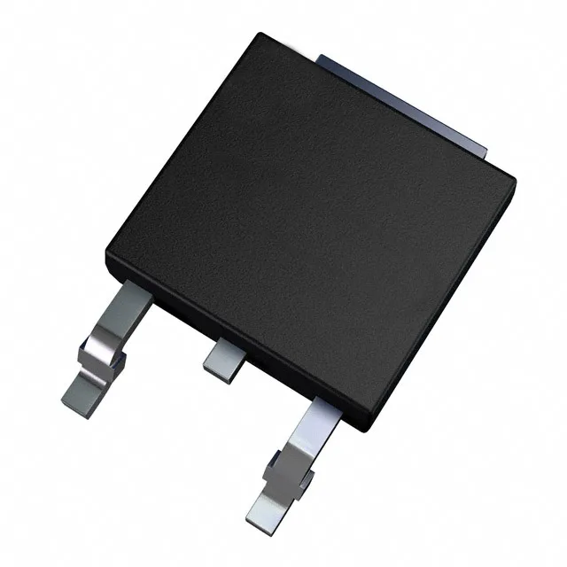
The STD30NE06LT4 is supplied in the DPAK package (TO-252-3, two leads plus tab). The supplier device package is DPAK, which is the standard surface-mount version of the TO-252 outline. The package is compatible with the standard TO-252 land pattern; no footprint deviation is required. The Tape & Reel (TR) packaging is the shipping medium, not a package variant — the device itself is the same DPAK case.