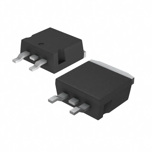
600 V N-channel MOSFET in D2PAK — switching converter fit
It is housed in a D2PAK (TO-263) surface-mount package, a standard footprint for medium-power, high-voltage switching stages in power supplies, adapters, and lighting ballasts.
On-resistance and gate charge — the switching loss trade-off
The low gate charge reduces the drive power required from the controller, a direct benefit in flyback and PFC stages operating above 65 kHz.
Thermal and input capacitance — layout and derating
Maximum power dissipation is 60 W at the case, with the junction temperature range spanning -55 to 150 °C. The input capacitance is 232 pF at 100 V drain-source, a figure that influences the drive circuit design and the switching node rise time.
It is ROHS3 compliant.