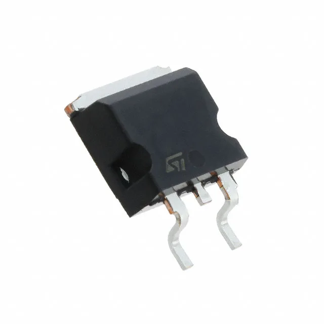
STMicroelectronics STB33N60DM6

STB33N60DM6 MOSFET N-CH 600V 25A D2PAK, 128mOhm

MPNSTB33N60DM6
End of Life

STMicroelectronics MDmesh™ M6 series, STB33N60DM6, N-Channel MOSFET, 600V Vdss, 25A Id, 128mOhm Rds(on) at 10V, 35nC Qg, D2PAK (TO-263), -55 to 150°C.

$5.69Ref. price · indicative, final on quote
PackagingTO-263-3, D²Pak (2 Leads + Tab), TO-263AB
RoHSROHS3 Compliant
SeriesMDmesh™ M6
Independent supplier — new & surplus stockAuthenticity-screened · ESD-safe packingListing updated Jul 2026

Specifications

STB33N60DM6 specifications
ParameterValue
SeriesMDmesh™ M6
FET typeN-Channel
MountingSurface Mount
Drain to source voltage600 V
Drive voltage (Max rds on, min rds on)10V
Current - continuous drain (Id) @ 25°C25A (Tc)
Power dissipation190W (Tc)
Operating temperature-55°C ~ 150°C (TJ)
PackageTape & Reel (TR); Cut Tape (CT)
Vgs±25V
TechnologyMOSFET (Metal Oxide)
CaseTO-263-3, D²Pak (2 Leads + Tab), TO-263AB
Vgs(th) (Max) @ id4.75V @ 250µA
Rds on (Max) @ id, vgs128mOhm @ 12.5A, 10V
Gate charge (Qg) (Max) @ vgs35 nC @ 10 V
Input capacitance (Ciss) (Max) @ vds1500 pF @ 100 V

Product details

600V, 25A, 128mOhm — the switching FET for a PFC or resonant converter

The STB33N60DM6 is an N-channel power MOSFET from ST's MDmesh™ M6 series, rated for 600 V drain-source breakdown and 25 A continuous drain current at 25°C case temperature. The on-resistance is 128 mOhm maximum at 12.5 A with a 10 V gate drive — the number that sets conduction losses in a hard-switched topology. Gate charge is 35 nC at 10 V, which keeps the gate-drive energy per cycle low enough that a standard bootstrap driver can handle it without excessive dissipation. Input capacitance at 100 V drain bias is 1500 pF, a figure that influences the switching transition time and the driver's peak current requirement. The part lives in a D2PAK (TO-263) surface-mount package with an exposed tab. That tab is the drain connection and must be soldered to a copper island on the PCB for thermal management — the package is rated for 190 W power dissipation at case temperature 25°C. The junction temperature range spans -55°C to 150°C, so it can sit in a hot industrial cabinet or an outdoor telecom rectifier without derating surprises.

What the gate charge and capacitance mean at the bench

A 35 nC total gate charge at 10 V means the driver needs to source and sink about 35 nC per switching cycle. The 1500 pF input capacitance at 100 V drain bias is the Ciss the driver sees during the Miller plateau.

Lifecycle and sourcing — active, no LTB watch

The STB33N60DM6 carries an Active product status and is ROHS3 compliant. There is no end-of-life notice or last-time-buy window to track. No second-source alternate is listed in the official record, but the D2PAK footprint is common across the MDmesh M6 family, so a pin-compatible density step (higher or lower Rds(on)) is a board-level option if the BOM needs flexibility.

Frequently asked questions

What is the Rds(on) of STB33N60DM6?

The maximum on-resistance is 128 mOhm at 12.5 A drain current with a 10 V gate drive. That is the spec to use for worst-case conduction loss calculations.

What is the direct replacement for STB33N60DM6?

No official direct replacement is listed in the manufacturer's documentation. The MDmesh M6 series includes other D2PAK devices with different Rds(on) and current ratings that share the same footprint — a density step is possible if the BOM allows a spec trade.

How does STB33N60DM6 compare to STB33N60M2?

The STB33N60M2 is an earlier MDmesh M2 generation part with the same voltage and current ratings but higher typical Rds(on) and gate charge. The M6 generation improves on-resistance and switching figures, which translates to lower conduction and switching losses in the same footprint. Exact numbers depend on the specific variant; check the respective datasheets for the delta.