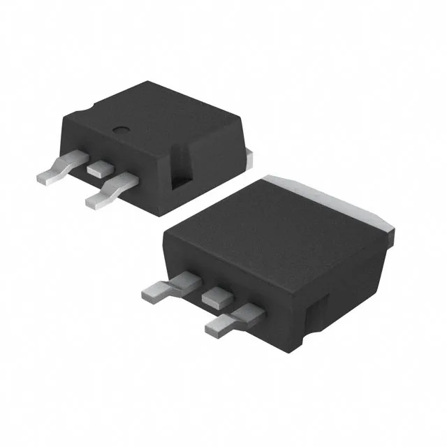
STMicroelectronics STB30NF10T4

STB30NF10T4 N-Channel MOSFET, 100V 35A D2PAK

MPNSTB30NF10T4
End of Life

STMicroelectronics STripFET™ II N-Channel MOSFET, STB30NF10T4, 100V Vdss, 35A Id, 45mOhm Rds(on), 55nC Qg, D2PAK (TO-263), -55°C to 175°C.

$1.75Ref. price · indicative, final on quote
PackagingTO-263-3, D²Pak (2 Leads + Tab), TO-263AB
RoHSROHS3 Compliant
SeriesSTripFET™ II
Independent supplier — new & surplus stockAuthenticity-screened · ESD-safe packingListing updated Jul 2026

Specifications

STB30NF10T4 specifications
ParameterValue
SeriesSTripFET™ II
FET typeN-Channel
MountingSurface Mount
Drain to source voltage100 V
Drive voltage (Max rds on, min rds on)10V
Current - continuous drain (Id) @ 25°C35A (Tc)
Power dissipation115W (Tc)
Operating temperature-55°C ~ 175°C (TJ)
PackageTape & Reel (TR); Cut Tape (CT)
Vgs±20V
TechnologyMOSFET (Metal Oxide)
CaseTO-263-3, D²Pak (2 Leads + Tab), TO-263AB
Vgs(th) (Max) @ id4V @ 250µA
Rds on (Max) @ id, vgs45mOhm @ 15A, 10V
Gate charge (Qg) (Max) @ vgs55 nC @ 10 V
Input capacitance (Ciss) (Max) @ vds1180 pF @ 25 V

Product details

100V, 35A N-channel in D2PAK

The STB30NF10T4: On-resistance is 45 mOhm maximum at 15 A drain current with a 10 V gate drive — this is the figure to use for conduction loss calculations in a synchronous rectifier or motor-drive output stage. Gate charge totals 55 nC at 10 V, so the driver must supply roughly 5.5 mA per 100 kHz of switching frequency just to charge the gate capacitance; the actual switching loss scales with the Qg × Vgs × fsw product.

Gate threshold and drive voltage

Input capacitance is 1180 pF typical at 25 V drain-source, which together with the gate charge sets the switching speed ceiling; the Miller plateau region is where the gate driver spends most of its time during the switching transition.

ROHS3 compliant per the manufacturer's declaration, with no lead, mercury, cadmium, or restricted phthalates in the package materials.

Frequently asked questions

Where can I buy STB30NF10T4 and check availability?

The STB30NF10T4 is an active-production part sourced through authorized and independent distribution channels.

What is the RDS(on) of STB30NF10T4?

Maximum on-resistance is 45 mOhm at 15 A drain current with a 10 V gate drive. This is the worst-case value across the operating temperature range; typical RDS(on) at 25°C is lower, but the 45 mOhm figure is the one to use for thermal design margin.

Is STB30NF10T4 a logic-level MOSFET?

No — the maximum gate threshold voltage is 4 V at 250 µA, and the recommended drive voltage for minimum on-resistance is 10 V.

What is the gate charge of STB30NF10T4?

Total gate charge is 55 nC at 10 V gate-source voltage. This value determines the gate-drive current required for a given switching frequency: at 100 kHz the average gate-drive current is 5.5 mA, and the peak current capability of the driver must be sufficient to charge the gate capacitance within the desired dead-time window.