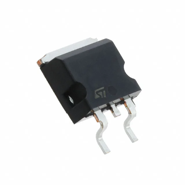
STMicroelectronics STB20N65M5

STB20N65M5 MOSFET N-Ch 650V 18A D2PAK, MDmesh V

MPNSTB20N65M5
End of Life

STMicroelectronics MDmesh™ V series, STB20N65M5, N-Channel MOSFET, 650 V Vdss, 18 A Id, 190 mOhm Rds(on) at 10 V, 36 nC Qg, D²PAK (TO-263) surface-mount package, 150 °C junction temperature.

$3.33Ref. price · indicative, final on quote
PackagingTO-263-3, D²Pak (2 Leads + Tab), TO-263AB
RoHSROHS3 Compliant
SeriesMDmesh™ V
Independent supplier — new & surplus stockAuthenticity-screened · ESD-safe packingListing updated Jul 2026

Specifications

STB20N65M5 specifications
ParameterValue
SeriesMDmesh™ V
FET typeN-Channel
MountingSurface Mount
Drain to source voltage650 V
Drive voltage (Max rds on, min rds on)10V
Current - continuous drain (Id) @ 25°C18A (Tc)
Power dissipation130W (Tc)
Operating temperature150°C (TJ)
PackageTape & Reel (TR); Cut Tape (CT)
Vgs±25V
TechnologyMOSFET (Metal Oxide)
CaseTO-263-3, D²Pak (2 Leads + Tab), TO-263AB
Vgs(th) (Max) @ id5V @ 250µA
Rds on (Max) @ id, vgs190mOhm @ 9A, 10V
Gate charge (Qg) (Max) @ vgs36 nC @ 10 V
Input capacitance (Ciss) (Max) @ vds1434 pF @ 100 V

Product details

Gate charge and switching behaviour

Input capacitance is 1434 pF at 100 V drain bias.

Thermal and package constraints

Maximum power dissipation is 130 W at case temperature, with the 150 °C junction temperature as the absolute limit. The D²PAK (TO-263) surface-mount package requires a copper land pattern on the PCB to sink heat — the tab area under the package sets the effective thermal resistance. For continuous operation near 18 A, a heatsink or forced airflow is assumed; at lower load currents the PCB copper alone may suffice.

Frequently asked questions

What is the Rds(on) of STB20N65M5?

Maximum on-resistance is 190 mOhm at 9 A drain current with 10 V gate drive. This is the value used for conduction-loss calculations at 25 °C junction; actual Rds(on) increases with temperature per the normalised curve in the datasheet.