What the 1200 V / 20 A rating means for your power stage
That 1200 V blocking voltage puts it squarely in high-voltage power conversion — think 800 V bus architectures in solar inverters, EV onboard chargers, and industrial motor drives where a 600 V MOSFET leaves no margin for switching transients. The 20 A continuous rating is at Tc=25°C; real-world derating follows the thermal curve, so a heatsink sized to keep the case below 100°C still delivers about 14 A usable.
With a maximum on-resistance of 290 mOhm at 10 A and 20 V gate drive, the SCT20N120 presents a conduction loss of about 2.9 W at that current — manageable with a modest heatsink. The total gate charge of 45 nC at 20 V means the gate driver only needs to source about 90 nC per switching cycle, keeping the drive loss low even at 50-100 kHz. Compare that to a similarly-rated superjunction MOSFET in the same TO-247 package: the SiC part typically halves the gate charge for the same Rds(on), which translates to lower driver losses and faster turn-on. The input capacitance of 650 pF at 400 V Vds is about a third of what an equivalent 600 V superjunction part would show, so the switching node rings less — you can often skip the snubber on the first prototype.
Thermal budget and package reality
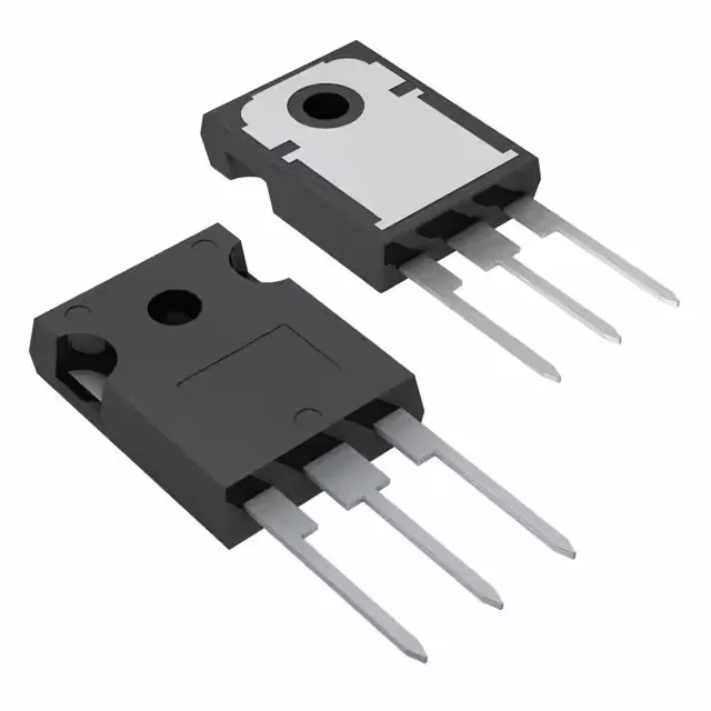
The TO-247-3 package (ST calls it HiP247™) is a through-hole, isolated-tab design — the metal tab is the drain, so you need an insulating pad and a thermal interface material if the heatsink is at chassis ground. Maximum power dissipation is 175 W at Tc=25°C, but that's the theoretical ceiling; in practice, a 40°C/W heatsink with forced air keeps the junction below 125°C at 3 A continuous. The 200°C Tj max is the absolute limit — stay below 175°C for long-term reliability, as the SiC body diode's reverse recovery degrades above that.
The ROHS3 compliance covers the EU directive for lead-free soldering.