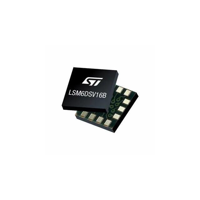
Triple-interface output — I²C, I3C, SPI
The LSM6DSV16BTR supports I²C, I3C℠, and SPI digital interfaces on the same die. I3C brings a backward-compatible upgrade path from I²C — the same two-wire bus, but with higher data rate and in-band interrupts — while SPI gives the lowest-latency streaming for a motion-capture or dead-reckoning pipeline. The interface choice is set at power-up by the CS pin and the bus configuration; a single PCB layout can serve all three protocols by populating the correct pull-up resistors.
6-axis inertial measurement with on-chip temperature
This is a 6-axis MEMS IMU — a 3-axis accelerometer and a 3-axis gyroscope in the same 14-LGA package — plus a temperature sensor for thermal compensation of the bias drift. The accelerometer and gyroscope share a common signal chain, so the cross-axis sensitivity and the alignment between the two sensing elements are calibrated at the factory. For a sensor-fusion algorithm running on the host MCU, the temperature output lets the firmware correct the gyro bias drift over the operating range without an external thermistor.
That means it can sit on a factory-floor sensor node that sees 60°C inside the enclosure on a summer afternoon, or on an outdoor IoT gateway that cycles through a -20°C night. The temperature sensor inside the package tracks the die temperature, not the ambient air — the firmware should use the sensor reading, not the ambient spec, for the bias-compensation algorithm.
14-LGA package — 2.5 mm × 3 mm footprint
The LSM6DSV16BTR comes in a 14-WFLGA package measuring 2.5 mm × 3 mm (supplier device package 14-LGA). The 0.5 mm pitch and the land-grid-array footprint keep the board area under 8 mm² — small enough for a wearable or a compact sensor module. The exposed pad on the bottom of the package is the thermal and mechanical ground; the PCB layout should connect it to the ground plane with at least four vias to pull heat from the MEMS die during high-ODR streaming.
Surface-mount assembly — Tape & Reel delivery
The 14-WFLGA package is compatible with lead-free reflow profiles per JEDEC J-STD-020. The reel quantity is the standard 7-inch reel for this package size — confirm the reel count with the RFQ for the BOM line quantity.