300 mA fixed 2.5 V LDO — PSRR and dropout for noise-sensitive rails
The LD39030SJ25R is a single-output linear regulator delivering 300 mA at a fixed 2.5 V from a maximum input of 5.5 V. PSRR is 62 dB from 1 kHz to 10 kHz — this flat band covers the switching frequencies of most upstream buck converters and charge pumps. For an analog supply rail feeding a 16-bit ADC or a precision op-amp, that rejection keeps ripple below the noise floor without an additional LC filter stage. Quiescent current is 50 µA typ, rising to 85 µA max. For always-on rails in battery-backed systems — RTC supplies, SRAM keep-alive, or sensor bias — that overhead is low enough to ignore in the sleep budget.
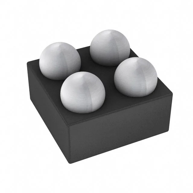
4-ball flip-chip — 0.79 mm × 0.79 mm footprint
The LD39030SJ25R comes in a 4-UFBGA/FCBGA package (4-Flipchip, 0.79×0.79 mm). The supplier device package is 4-Flipchip with a 0.79×0.79 mm body — the same as the package/case designation. This is a wafer-level chip-scale package (WLCSP); the solder balls are directly on the die pads, so the board footprint is essentially the die size plus the ball pitch. Surface-mount assembly with standard lead-free reflow profiles applies. No underfill is required for typical handheld or IoT use, but if the board sees repetitive thermal cycling or mechanical shock (portable instruments, automotive modules), a capillary underfill under the 0.79 mm body improves solder-joint life.
Active production — no LTB window open
Protection features include over-current, over-temperature, and soft-start, so the part handles start-up into a discharged output capacitor without current spikes.