80 V, 1.5 A NPN — linear and switching duty
The BD139-10 is an NPN epitaxial planar transistor rated for 80 V collector-emitter breakdown and 1.5 A continuous collector current. It is specified for general-purpose linear amplifier and low-to-medium speed switching applications where a through-hole package and moderate power dissipation are acceptable. Maximum power dissipation is 1.25 W, which sets the thermal budget for continuous operation in the TO-225AA / SOT-32 package. The junction temperature rating of 150 °C defines the safe operating area; derating is required above 25 °C ambient.
Saturation voltage and DC gain — drive margin check
Vce(sat) is specified at 500 mV maximum with 50 mA base current driving 500 mA collector current. This saturation voltage is the conduction loss floor in a low-side switch or linear regulator pass element. The gain at the operating point determines the base drive current required to keep the transistor in saturation; a lower hFE demands more base current from the driving stage. Collector cutoff current is 100 nA maximum (ICBO), which is low enough for most linear circuits but should be considered in high-impedance bias networks at elevated temperature.
Through-hole SOT-32 — board integration
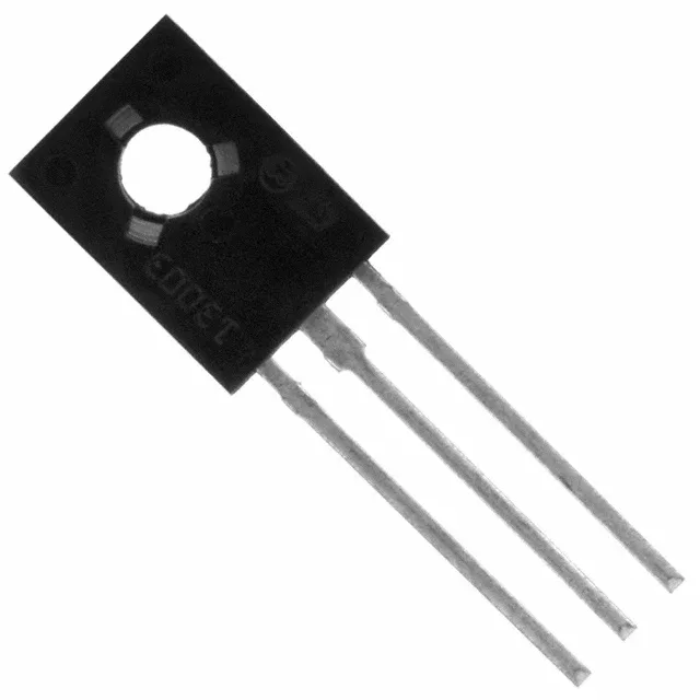
The BD139-10 is supplied in a through-hole SOT-32 package (also designated TO-225AA or TO-126-3). The three-lead, tabbed package is designed for vertical mounting on a PCB or heatsink; the metal tab provides a low-thermal-resistance path to the ambient or a clip-on heatsink.